Preparation method of MEMS formaldehyde sensor based on aluminum-doped zinc oxide porous nano-film
A technology of aluminum-doped zinc oxide and formaldehyde sensors, which is applied in the field of formaldehyde sensors, can solve the problems of increasing process implementation, increasing film damage, increasing process steps, etc., and achieves the effects of improving test stability, improving response, and increasing contact area
- Summary
- Abstract
- Description
- Claims
- Application Information
AI Technical Summary
Problems solved by technology
Method used
Image

Examples
Embodiment 1
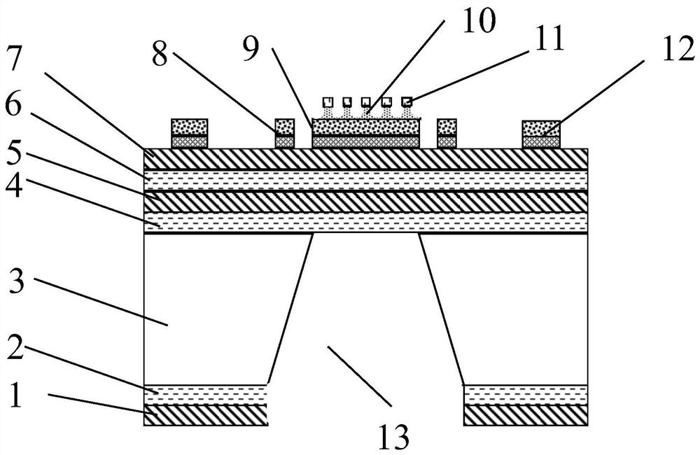
[0085] (1) As shown in Figure 8(a), the first layer of SiO was prepared on the upper and lower sides of the Si substrate by thermal oxidation. 2 insulating layer and the first layer of SiO 2 masking layer, in the first layer SiO 2 insulating layer and the first layer of SiO 2 The first layer of Si was prepared respectively on the masking layer 3 N 4 insulating layer and Si 3 N 4 masking layer, where SiO 2 layer film thickness is 500nm, Si 3 N 4 The thickness of the layer is 150 nm.
[0086] (2) As shown in Figure 8(b), in the first layer of Si 3 N 4 The second layer of SiO was sequentially prepared on the insulating layer 2 insulating layer and second layer Si 3 N 4 Insulation layer, put the silicon wafer into the tube annealing furnace, set the temperature at 500°C, and pass 100% N for 1 hour first 2 , followed by 5 hours of 6% O 2 , ultimatum 1 hour 100% N 2 Anneal for 5 hours.
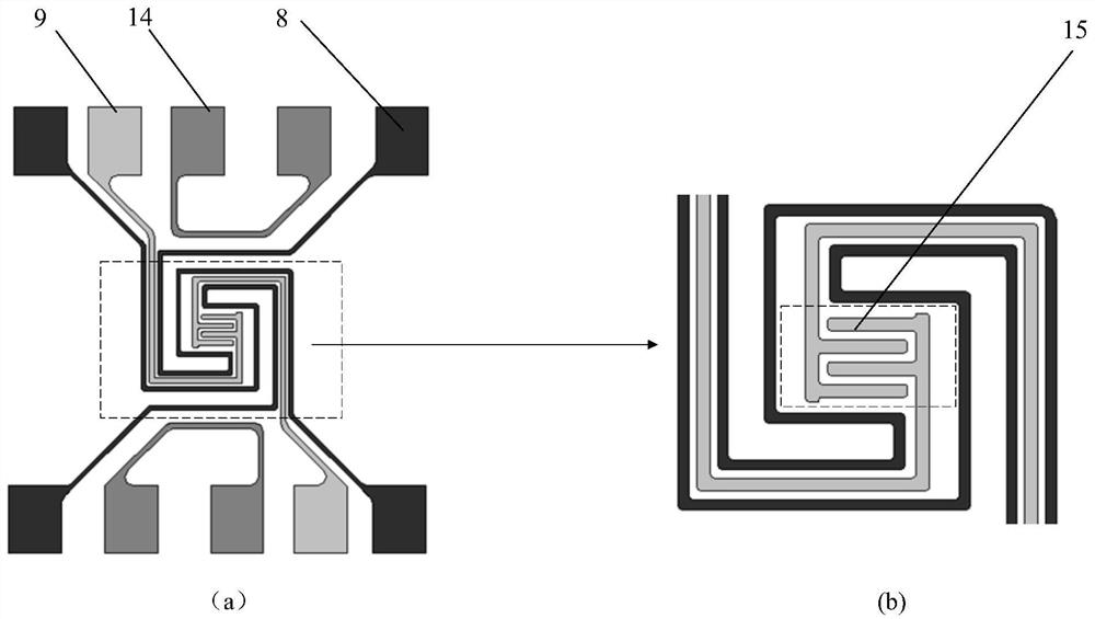
[0087] (3) As shown in Figure 8(c), the second layer of Si on the front support...
Embodiment 2
[0103] (1) As shown in Figure 8(a), the first layer of SiO was prepared on the upper and lower sides of the Si substrate by thermal oxidation. 2 insulating layer and the first layer of SiO 2 masking layer, in the first layer SiO 2 insulating layer and the first layer of SiO 2 The first layer of Si was prepared respectively on the masking layer 3 N 4 insulating layer and Si 3 N 4 masking layer, forming SiO 2 -Si 3 N 4 The front support layer film and the back mask layer film; where SiO 2 layer film thickness is 490nm, Si 3 N 4 The thickness of the layer is 140 nm.
[0104] (2) As shown in Figure 8(b), in the first layer of Si 3 N 4 The second layer of SiO was sequentially prepared on the insulating layer 2 insulating layer and second layer Si 3 N 4 Insulation layer, put the silicon wafer into the tube annealing furnace, set the temperature at 600°C, and pass 100% N for 1 hour first 2 , followed by 3 hours of 5% O 2 , ultimatum 1 hour 100% N 2 Anneal for 7 hou...
Embodiment 3
[0121] (1) As shown in Figure 8(a), the first layer of SiO was prepared on the upper and lower sides of the Si substrate by thermal oxidation. 2 insulating layer and the first layer of SiO 2 masking layer, in the first layer SiO 2 insulating layer and the first layer of SiO 2 The first layer of Si was prepared respectively on the masking layer 3 N 4 insulating layer and Si 3 N 4 masking layer, forming SiO 2 -Si 3 N 4 The front support layer film and the back mask layer film; where SiO 2 Layer film thickness is 510nm, Si 3 N 4 The thickness of the layer is 160 nm.
[0122] (2) As shown in Figure 8(b), in the first layer of Si3 N 4 The second layer of SiO was sequentially prepared on the insulating layer 2 insulating layer and second layer Si 3 N 4 Insulation layer, put the silicon wafer into the tube annealing furnace, set the temperature at 550°C, and pass 100% N for 1 hour first 2 , followed by 5 hours of 5% O 2 , ultimatum 1 hour 100% N 2 Anneal for 5 hours...
PUM
| Property | Measurement | Unit |
|---|---|---|
| Diameter | aaaaa | aaaaa |
| Thickness | aaaaa | aaaaa |
| Thickness | aaaaa | aaaaa |
Abstract
Description
Claims
Application Information
 - R&D Engineer
- R&D Manager
- IP Professional
- Industry Leading Data Capabilities
- Powerful AI technology
- Patent DNA Extraction
Browse by: Latest US Patents, China's latest patents, Technical Efficacy Thesaurus, Application Domain, Technology Topic.
© 2024 PatSnap. All rights reserved.Legal|Privacy policy|Modern Slavery Act Transparency Statement|Sitemap