Eureka AIR delivers breakthrough ideas for toughest innovation challenges, trusted by R&D personnel around the world.

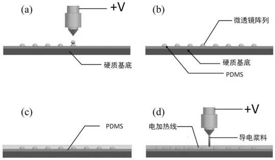
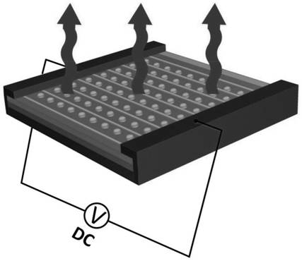
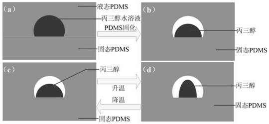
A method of manufacturing an embedded self-defogging and zooming microlens array, its product and its application

A micro-lens array, embedded technology, applied in lenses, manufacturing, manufacturing tools, etc., can solve problems such as difficult to achieve rapid zoom, fogging, icing, etc. simple steps

Active Publication Date: 2022-03-01
QINGDAO TECHNOLOGICAL UNIVERSITY
View PDF4 Cites 0 Cited by
  • Summary
  • Abstract
  • Description
  • Claims
  • Application Information

AI Technical Summary

Problems solved by technology

However, in view of the problems that the microlens array is prone to fogging, frosting or even icing in the application process of extreme strips, and it is difficult to achieve fast zooming, it is urgent to develop a new microlens array structure and processing technology to achieve automatic defogging and zooming. Low-cost, mass production of microlens arrays

Method used


Image

  • A method of manufacturing an embedded self-defogging and zooming microlens array, its product and its application
  • A method of manufacturing an embedded self-defogging and zooming microlens array, its product and its application
  • A method of manufacturing an embedded self-defogging and zooming microlens array, its product and its application

Examples


Embodiment 1

[0044] Step 1: Prepare the printing substrate

[0045] (1) Choose ordinary glass as the hard substrate, first place the ordinary glass in isopropanol solution for ultrasonic cleaning for 5 minutes, then place it in deionized water for ultrasonic cleaning for 5 minutes, and finally dry it with nitrogen, take it out for use;

[0046] (2) The PDMS liquid is Sylgard 184 from Dow Corning Company, and the PDMS elastomer and its corresponding curing agent are stirred and mixed evenly at a mass ratio of 10:1, and placed in a vacuum drying oven to evacuate to remove air bubbles;

[0047] (3) Pour the vacuum-treated PDMS liquid on the surface of ordinary glass, let it stand for 2 minutes, and then place it on a coater for spin coating. The spin coating time is 2 minutes, and the rotation speed is 500r / min to form a layer of PDMS liquid about 50 μm thick. Finally, place it in a vacuum drying oven and heat it at 70°C for 30 minutes, the PDMS will be cross-linked and cured by heating, and ...

Embodiment 2

[0056] Step 1: Prepare the printing substrate

[0057] (1) Choose a silicon wafer as the hard substrate, first clean the silicon wafer with isopropanol solution for 5 minutes, then place it in deionized water for 5 minutes to remove the residual isopropanol solution, and finally dry it with nitrogen, take it out for use ;

[0058] (2) Select Sylgard 184 from Dow Corning as the PDMS liquid, stir and mix the PDMS elastomer and curing agent at a ratio of 10:1, and place in a vacuum drying oven to evacuate to remove air bubbles;

[0059] (3) Pour the vacuum-treated PDMS liquid on the surface of the silicon wafer, spin-coat it with a coating machine, spin-coat for 2 minutes, and rotate at a speed of 500r / min to form a layer of PDMS liquid about 50 μm thick; finally place it in vacuum drying Heating in the box at 75°C for 30 minutes, the PDMS is heated to cross-link and solidify, and the printing substrate is prepared;

[0060] Step 2: Print Microlens Array

[0061] (1) Select 60...

Embodiment 3

[0071] Step 1: Prepare the printing substrate.

[0072] (1) Select high-quality float glass as the hard substrate, first place the float glass in isopropanol solution for ultrasonic cleaning for 5 minutes, then place it in deionized water for ultrasonic cleaning for 5 minutes, and finally dry it with nitrogen, take it out for use;

[0073] (2) The PDMS liquid is Sylgard 184 from Dow Corning Company. The PDMS elastomer and its corresponding curing agent are stirred and mixed evenly at a ratio of 10:1, and placed in a vacuum drying oven to evacuate to remove air bubbles;

[0074] (3) Pour the vacuum-treated PDMS liquid on the surface of the float glass, let it stand for 2 minutes, and then place it on a homogenizer for spin coating. The spin coating time is 1 min, and the speed is 500r / min to form a layer of PDMS liquid about 80 μm thick. . Finally, it was placed in a vacuum drying oven and heated at 75°C for 30 minutes. The PDMS was heated to cross-link and solidify, and the pri...


PUM

PropertyMeasurementUnit
widthaaaaaaaaaa
widthaaaaaaaaaa
widthaaaaaaaaaa

Abstract

The invention provides a manufacturing method, product and application of an embedded self-defogging and zooming microlens array. This method not only realizes the ultra-high resolution embedded microlens array manufacturing, but also fills the gaps of the microlens array with transparent electrodes, and uses the Joule heat generated after the transparent electrodes are electrified to realize the function of automatic defogging. The array material adopts liquid material and is encapsulated in the microhole array, and the contact angle of the droplet can be changed through the electric heating of the transparent electrode to realize the zooming of the microlens array.

Description

technical field [0001] The invention belongs to the field of optical manufacturing, and in particular relates to a preparation method, product and application of a microlens array capable of automatically defogging. Background technique [0002] The microlens array is an array formed by microlenses with a diameter between 10 μm and 1 mm according to a certain arrangement and combination. It has broad application prospects in the fields of displays, endoscopes, panoramic cameras, microsensors, and optical communications. At present, with the rapid development of manufacturing technology, a variety of manufacturing technologies of microlens arrays have emerged, the representative ones are microjet printing method, photolithography hot melting method, electrowetting method, femtosecond laser direct writing method, femto Second laser acid etching method, self-assembly method, molding method, hot pressing method and mechanical processing method, etc., even in the performance of m...

Claims


Application Information

Patent Timeline
Patent Type & Authority Patents(China)
IPC IPC(8): B29C64/106B29C64/30B29C64/314G02B3/14B33Y10/00B33Y40/10B33Y40/20
CPCB29C64/106B29C64/30B29C64/314G02B3/14B33Y10/00B33Y40/10B33Y40/20
Inventor 朱晓阳李政豪兰红波李红珂孙銮法杨建军
Owner QINGDAO TECHNOLOGICAL UNIVERSITY
Why Eureka
Eureka Blog
Learn More