

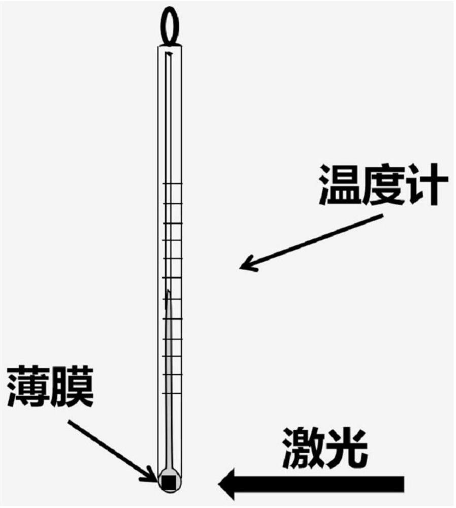
Method for preparing nano-film based on infrared photothermal conversion and measuring light power
A nano-thin film and thermal conversion technology, which is used in photometry using electrical radiation detectors, metal selenide/telluride, binary selenium/tellurium compounds, etc. The problems of small space optical power and inconvenient continuous power supply have achieved the effects of low equipment requirements, single shape and short response time.
- Summary
- Abstract
- Description
- Claims
- Application Information
AI Technical Summary
Problems solved by technology
Method used
Image

Examples
preparation example Construction
[0031] A method for preparing a nano-film based on infrared photothermal conversion, the specific steps are:
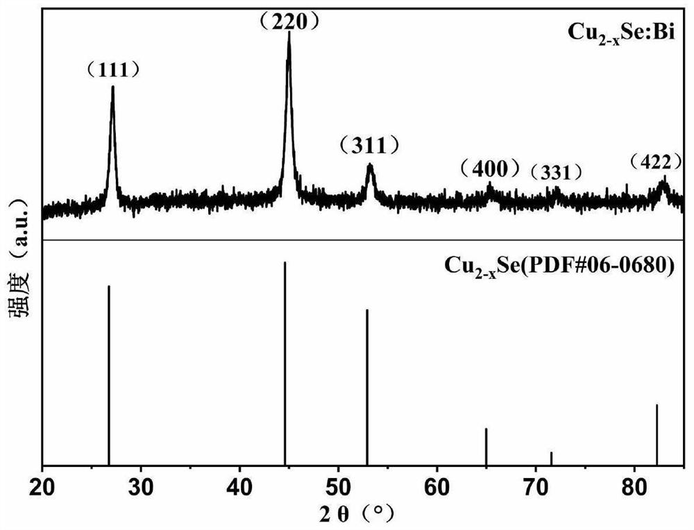
[0032] S1, Cu 2-x Preparation of Se:Bi Nanocrystalline Powder
[0033] With ethylene glycol as solvent, with Na 2 SeO 3 As the selenium source, take CuCl 2 2H 2 O is copper source, wherein the molar ratio of copper source and selenium source is 2:1, adjust pH value with NaOH, take Bi(NO 3 ) 3 ·5H 2 O is a bismuth source, adding PVP is a stabilizer, and stirs evenly;
[0034] The stirred mixture was transferred to a microwave system, and microwaved at 180°C to obtain Cu-containing 2-x Se:Bi nanocrystal solution, the solution is washed and dried to obtain Cu 2-x Se: Bi nanocrystalline powder;
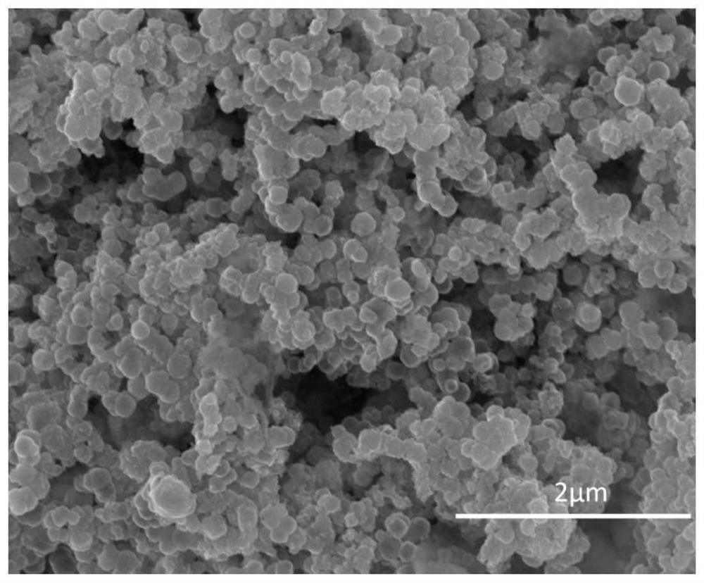
[0035] S2, Cu 2-x Preparation of Se:Bi Nanocrystalline Thin Films
[0036] With water as solvent, with the Cu prepared in step S1 2-x Se:Bi nanocrystalline powder is a solute, which is dissolved under the action of ultrasonic waves. 2-x Se:Bi nanocrystalline particl...
specific Embodiment
[0048] 0.1343g of Na 2 SeO 3 , 0.2645g of CuCl 2 2H 2 O, 0.0388g of Bi(NO 3 ) 3 ·5H 2 O, the NaOH of 0.1690g, the PVP of 0.3121g and the ethylene glycol of 40ml join in the three-necked bottle of 100ml, the three-necked bottle that is filled with mixed solution is transferred in the microwave system and carries out magnetic stirring, 300 rev / mins of rotating speed, After 30 minutes, the magnetic stirring speed was adjusted to 100 rpm, and microwave reaction was carried out at 180°C for 15 minutes to obtain Cu-containing 2-x Se:Bi nanocrystal solution, the resulting solution was transferred to a dry and clean centrifuge tube and centrifuged at a speed of 10000 rpm for 10min, and the precipitate obtained by centrifugation was washed three times with deionized water and absolute ethanol, and then transferred to a petri dish at room temperature. Dry and collect the powder, which is Cu 2-x Se:Bi nanocrystalline powder.
[0049] Will get Cu 2-x Se:Bi nanocrystalline powder ...
PUM
| Property | Measurement | Unit |
|---|---|---|
| diameter | aaaaa | aaaaa |
| wavelength | aaaaa | aaaaa |
Abstract
Description
Claims
Application Information