Lithium niobate optical sensor and method based on Bloch surface waves
An optical sensor, lithium niobate technology, applied in the field of optical technology science, can solve the problems of low sensor sensitivity and only sensor sensitivity, and achieve the effect of simple production, real-time and repeatable detection
- Summary
- Abstract
- Description
- Claims
- Application Information
AI Technical Summary
Problems solved by technology
Method used
Image
Examples
Embodiment 1
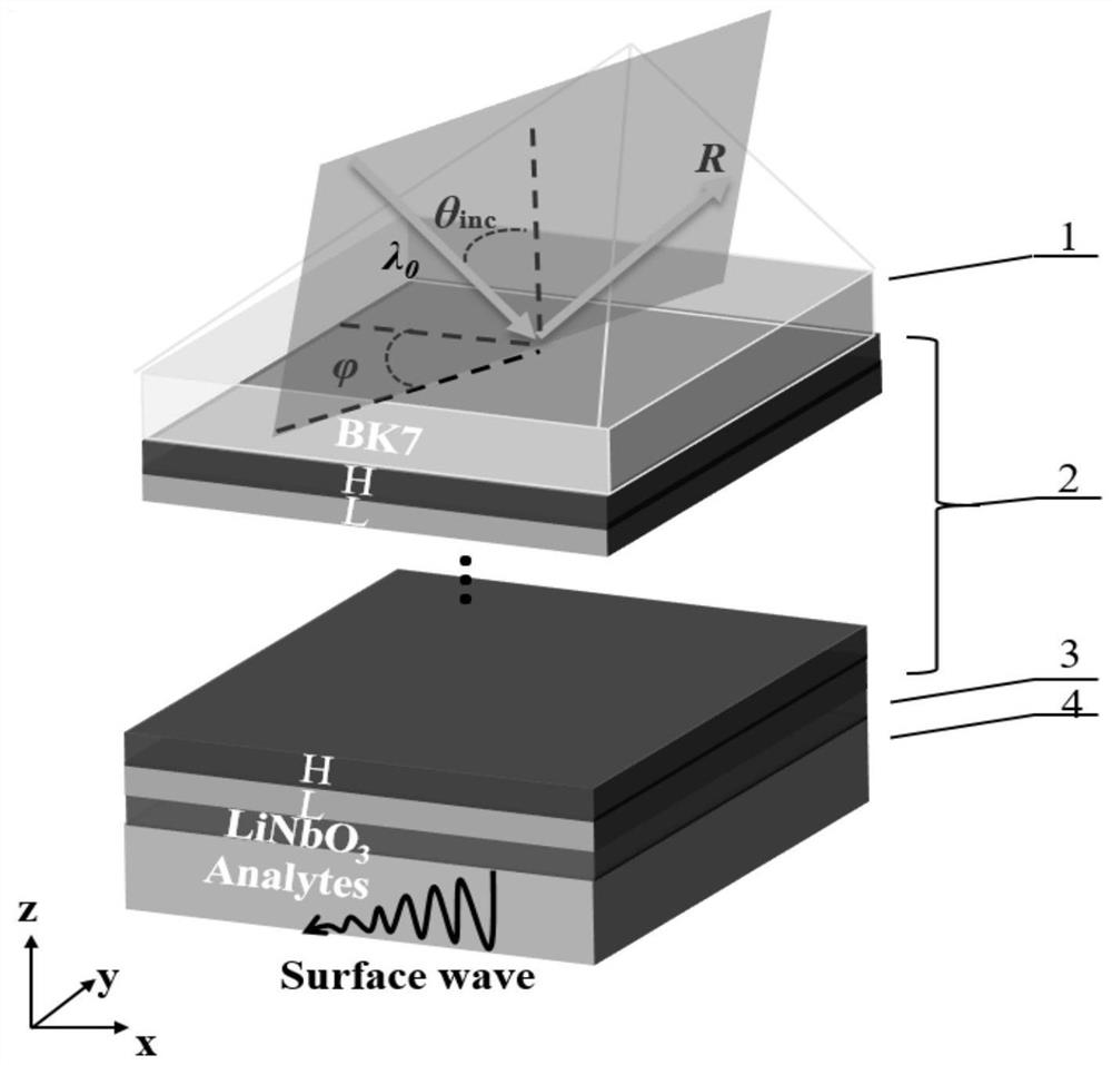
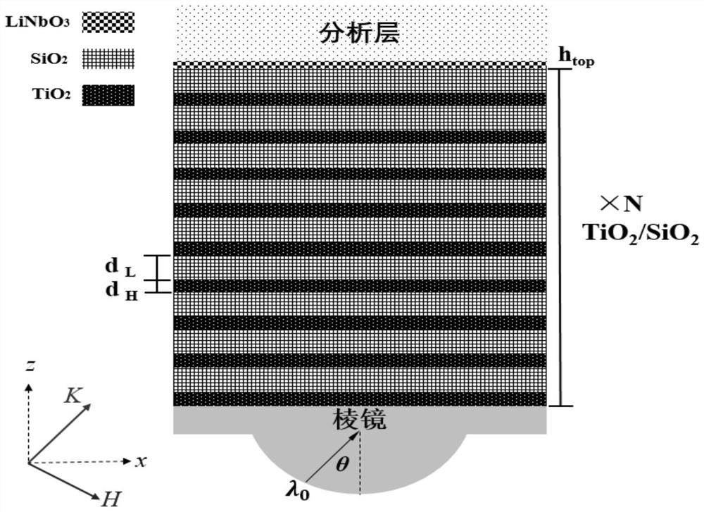
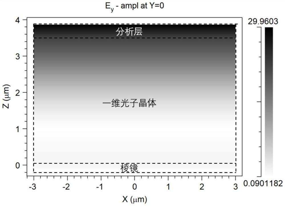
[0035] In this example, the high refractive index material in the periodic photonic crystal 2 selects n H = 2.15 titanium dioxide (TiO 2 ), the low refractive index material is selected with a refractive index n L =1.32 silicon dioxide (SiO 2 ), the periodic photonic crystal 2 is formed by periodic arrangement of titanium dioxide and silicon dioxide, and the thickness is d H = 151nm and d L =246nm, periodicity N=9. The defect layer consists of thickness h Top =55nm lithium niobate absorption medium composition. The overall structure of the device is: BK7 prism - one-dimensional photonic crystal - lithium niobate defect layer - sample layer to be tested. In this case we set the refractive index of the external medium around its initial value n air The change of = 1.001 (air) was detected and analyzed by passing the gas through the microfluidic device and flowing over the sensor surface. The wavelength interrogation method is adopted, that is, a fixed incident angle of 4...
Embodiment 2
[0037] In this example, the high refractive index material H in the periodic photonic crystal 2 selects n H = 2.15 titanium dioxide (TiO 2 ), the low refractive index material L selects the refractive index n L =1.32 silicon dioxide (SiO 2 ), the periodic photonic crystal 2 is formed by periodic arrangement of titanium dioxide and silicon dioxide, and the thickness is d H = 151nm and d L =246nm, periodicity N=9. The defect layer consists of thickness h Top =55nm lithium niobate absorption medium composition. The overall structure of the device is: BK7 prism - one-dimensional photonic crystal - lithium niobate defect layer - sample layer to be tested. In this case we set the refractive index of the external medium around its initial value n air The change of = 1.001 (air) was detected and analyzed by passing the gas through the microfluidic device and flowing over the sensor surface. The azimuth interrogation method is adopted, that is, a fixed incident angle of 44.97° ...
PUM
| Property | Measurement | Unit |
|---|---|---|
| thickness | aaaaa | aaaaa |
| thickness | aaaaa | aaaaa |
| thickness | aaaaa | aaaaa |
Abstract
Description
Claims
Application Information


