Preparation method of weak light type copper indium gallium selenide solar cell applied indoors
A solar cell, copper indium gallium selenide technology, applied in photovoltaic power generation, circuits, electrical components, etc., can solve the problems of low photoelectric conversion efficiency of cells, unstable power generation of amorphous silicon weak light solar cells, and weak illuminance, etc., and achieve improvement. Indoor power generation efficiency, improving photoelectric conversion efficiency, increasing absorption and utilization effects
- Summary
- Abstract
- Description
- Claims
- Application Information
AI Technical Summary
Problems solved by technology
Method used
Image

Examples
Embodiment approach
[0045] A method for preparing a low-light copper indium gallium selenide solar cell for indoor application, comprising the following steps:
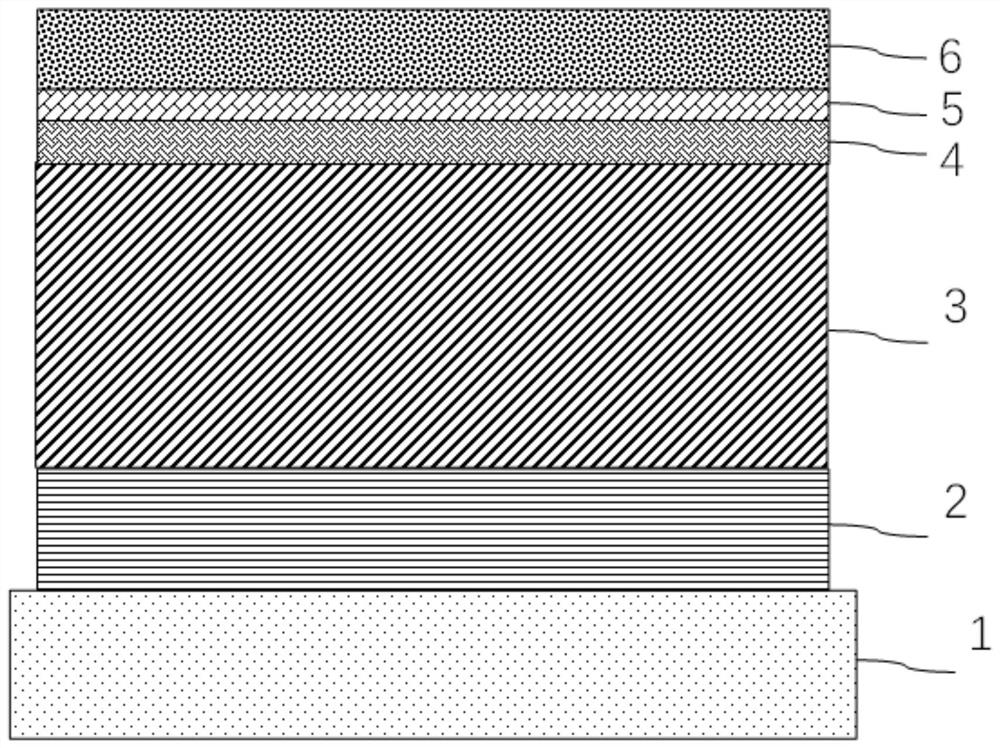
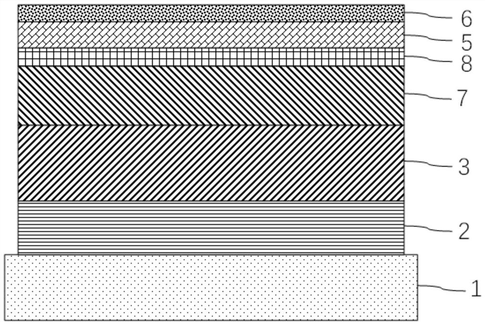
[0046] (1) Deposit Mo back electrodes on glass substrates or flexible substrates using DC magnetron sputtering; the thickness of Mo back electrodes is 450-550 nm.
[0047] (2) Deposit the NaF pre-layer on the Mo back electrode first, and then deposit the CIGS light-absorbing layer. Depositing the NaF preset layer is specifically: at a vacuum degree of 1-3×10 -3 Raise the substrate temperature to 150-300°C in the co-evaporation chamber of Pa, co-evaporate a layer of NaF on the surface of the Mo back electrode, the temperature of the NaF evaporation source is 760-800°C, and the evaporation time is 10-20min.
[0048] Co-evaporation deposition of CIGS light absorbing layer comprises the following steps:
[0049] The first step: co-evaporating copper, indium, gallium, and selenium metal sources to form a P-type CIGS light absorption layer w...
Embodiment 1
[0057] A Mo back electrode with a thickness of 500 nm was deposited on the soda lime silica glass substrate by DC magnetron sputtering.
[0058] In a vacuum of 1×10 -3 Raise the substrate temperature to 270°C in the co-evaporation chamber of Pa, and co-evaporate a NaF layer on the surface of the Mo back electrode. The NaF evaporation source temperature is 775°C, and the evaporation time is 10min.
[0059] The first step of co-evaporation: raise the temperature of the substrate to 500°C, the temperature of the In evaporation source is 1020°C, the temperature of the Ga evaporation source is 1160°C, the temperature of the Cu evaporation source is 1360°C, the temperature of the Se evaporation source is 480°C, and the evaporation time is 20min. During the evaporation process, the metal source evaporation ratio Cu / (Ga+In) was kept at 0.88, Ga / (Ga+In) at 0.42, and the evaporation thickness was controlled at 1.2 μm.
[0060] The second step of co-evaporation: keep the substrate temp...
Embodiment 2
[0066] A Mo back electrode with a thickness of 550 nm was deposited on a stainless steel substrate by DC magnetron sputtering.
[0067] In a vacuum of 1×10 -3 Raise the substrate temperature to 300°C in the co-evaporation chamber of Pa, and co-evaporate a layer of NaF on the surface of the Mo layer. The temperature of the NaF evaporation source is 760°C, and the evaporation time is 15 minutes.
[0068] The first step of co-evaporation: raise the temperature of the substrate to 520°C, the temperature of the In evaporation source is 1000°C, the temperature of the Ga evaporation source is 1175°C, the temperature of the Cu evaporation source is 1375°C, the temperature of the Se evaporation source is 470°C, and the evaporation time is 23min. During the evaporation process, the metal source evaporation ratio Cu / (Ga+In) was kept at 0.87, Ga / (Ga+In) at 0.45, and the evaporation thickness was controlled at 1.3 μm.
[0069] The second step of co-evaporation: keep the substrate tempera...
PUM
| Property | Measurement | Unit |
|---|---|---|
| Thickness | aaaaa | aaaaa |
| Thickness | aaaaa | aaaaa |
| Deposition thickness | aaaaa | aaaaa |
Abstract
Description
Claims
Application Information
 - R&D
- Intellectual Property
- Life Sciences
- Materials
- Tech Scout
- Unparalleled Data Quality
- Higher Quality Content
- 60% Fewer Hallucinations
Browse by: Latest US Patents, China's latest patents, Technical Efficacy Thesaurus, Application Domain, Technology Topic, Popular Technical Reports.
© 2025 PatSnap. All rights reserved.Legal|Privacy policy|Modern Slavery Act Transparency Statement|Sitemap|About US| Contact US: help@patsnap.com