High-stability temperature sensor for body temperature monitoring and preparation method thereof
A temperature sensor, high-stability technology, used in thermometers using directly heat-sensitive electrical/magnetic components, nanotechnology for sensing, body temperature measurement, etc., can solve the problem of high device cost, low sensitivity, and device life. It can achieve the effect of simple preparation process, low cost and reducing the density of defect states.
- Summary
- Abstract
- Description
- Claims
- Application Information
AI Technical Summary
Problems solved by technology
Method used
Image
Examples
Embodiment 1
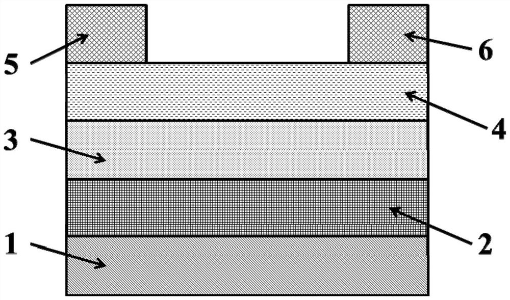
[0036] A high-stability temperature sensor for body temperature monitoring provided by a preferred embodiment of the present invention includes a substrate, a gate electrode, a gate insulating layer, an organic semiconductor, a source electrode and a drain electrode, and the organic semiconductor layer introduces The mass fraction is 1%-3% soybean isoflavone and 0.2%-0.5% dibutyl hydroxytoluene.
[0037]The substrate can be a rigid substrate or a flexible substrate, such as one of silicon wafer, glass, polymer film and metal foil, which has a certain ability of waterproofing and oxygen penetration, and has better surface smoothness.
[0038] The gate electrode, source electrode, and drain electrode are made of materials with low resistance, such as gold (Au), silver (Ag), magnesium (Mg), aluminum (Al), copper (Cu), calcium (Ca), barium (Ba ), nickel (Ni) and other metals and their alloy materials, metal oxides, such as indium tin oxide (ITO), zinc tin oxide (IZO) conductive fi...
Embodiment 2
[0043] In this embodiment, on the basis of Embodiment 1, the preparation method is as follows:
[0044] ① Thoroughly clean the glass substrate on which the gate electrode ITO has been sputtered, and dry it with dry nitrogen after cleaning;
[0045] ② Prepare a PS film on ITO by spin coating to form a gate insulating layer of 100nm;
[0046] ③The spin-coated PS film is heated and baked;
[0047] ④ Spin-coat a 100nm mixed organic semiconductor layer of P3HT, soybean isoflavone, and dibutyl hydroxytoluene with a mass fraction of 98.5%: 1%: 0.5% on the gate insulating layer;
[0048] ⑤ Copper source electrode and drain electrode 100nm were prepared by vacuum evaporation.
[0049] The temperature response characteristics of the device are tested, and the detection effect is good and the service life is long.
Embodiment 3
[0051] In this embodiment, on the basis of Embodiment 1, the preparation method is as follows:
[0052] ① Thoroughly clean the glass substrate 1 on which the gate electrode ITO has been sputtered, and dry it with dry nitrogen after cleaning;
[0053] ② Prepare a PVA film on ITO by spin coating method to form a 20nm gate insulating layer;
[0054] ③The spin-coated PVA film is heated and baked;
[0055] ④ Spin-coat a 200nm mixed organic semiconductor layer of P3HT, soybean isoflavone, and dibutyl hydroxytoluene with a mass fraction of 96.8%: 3%: 0.2% on the gate insulating layer;
[0056] ⑤ Prepare gold source electrode and drain electrode 40nm by vacuum evaporation.
[0057] The temperature response characteristics of the device are tested, and the detection effect is good and the service life is the longest.
PUM
| Property | Measurement | Unit |
|---|---|---|
| thickness | aaaaa | aaaaa |
| thickness | aaaaa | aaaaa |
| thickness | aaaaa | aaaaa |
Abstract
Description
Claims
Application Information
