Phase change memory based on nano current channel

A phase change memory and current channel technology, applied in the field of phase change memory, can solve the problems of high difficulty and high process cost, and achieve the effects of reducing device power consumption, simple process and improving current density

Active Publication Date: 2021-04-23
HUAZHONG UNIV OF SCI & TECH
View PDF17 Cites 2 Cited by
  • Summary
  • Abstract
  • Description
  • Claims
  • Application Information

AI Technical Summary

Problems solved by technology

[0007] Aiming at the defects of the prior art, the present invention provides a phase-change memory based on a nano-current channel, the purpose of which is to solve the problem of high process cost and difficulty in reducing writing power consumption by changing the structure of the existing device, and Increase the current density in the contact area, improve the heat generation efficiency, and improve the heat utilization efficiency, so that the phase change memory can reduce the write power consumption without reducing the cell size and without improving the process.

Method used


Image

  • Phase change memory based on nano current channel
  • Phase change memory based on nano current channel
  • Phase change memory based on nano current channel

Examples


preparation example Construction

[0054] According to another aspect of the present invention, the present invention provides a nano current channel layer and a method for preparing a phase change memory containing a nano current channel layer, which is characterized in that magnetron sputtering, chemical vapor deposition, plasma enhanced chemical Any of vapor deposition, physical vapor deposition, laser pulse deposition, evaporation, electrochemical growth, ion implantation, molecular beam epitaxy, atomic vapor deposition, and atomic layer deposition.

[0055] The present invention also provides a preparation method of a phase-change memory based on a nano-current channel. power consumption purposes.

Embodiment 1

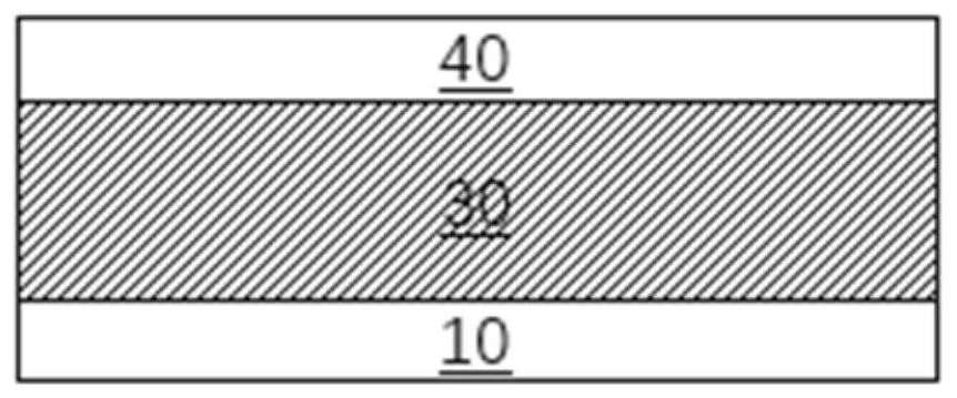
[0058] According to the first embodiment of the present invention, the sectional view of an exemplary structure of a conventional phase-change memory is as follows: figure 1 show.

[0059] The bottom electrode 10 is formed on SiO 2 On the substrate, the material of the bottom electrode 10 is selected from W, Pt, Au, Al, Cu, Ti, Ta and other metal materials and conductive materials of their alloys. A phase change material layer 30 is formed on the bottom electrode 10, and the phase change layer material 30 includes a chalcogenide compound. Preferably, the chalcogenide compound includes an alloy compound formed by one of S, Se, Te and other non-chalcogenide materials, wherein the non-chalcogenide material includes Ge, Sb, Ga, Bi, In, Sn, Pb, Ag, N, One or more of O; preferably, the chalcogenides include GeTe, GeSb, Ge 2 Sb 2 Te 5 、 Ge 1 Sb 2 Te 4 , Sb 2 Te 3 , AgInSbTe; more preferably, the chalcogenide compound includes a compound formed by doping and modifying the ab...

Embodiment 2

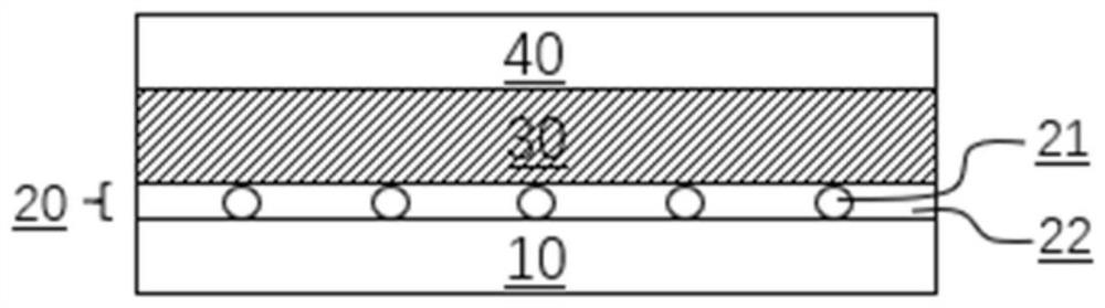
[0063] According to the second embodiment of the present invention, the finite element simulation is performed on the phase-change memory structure with the nano current channel layer and the writing process of the traditional phase-change memory structure.

[0064] The simulation adopts the simplest three-layer phase-change memory cell structure in Embodiment 1. The material parameters used in the simulation are listed in Table 1 (the thermal and electrical parameters of various materials used in the finite element analysis). The upper and lower electrodes of the two cell structures are made of Pt, and the insulating material between the cells is SiO 2 And the phase change layer material is Ge2 Sb 2 Te 5 , the thickness of the upper and lower electrodes, insulating layer, and phase change layer are all 100nm, and the diameter of the unit device is 100nm. In the structure with a nano-current channel layer, the thickness of the nano-current channel layer is set to 5nm. SiO 2...


PUM

PropertyMeasurementUnit
thicknessaaaaaaaaaa
sizeaaaaaaaaaa
thicknessaaaaaaaaaa

Abstract

The invention discloses a phase change memory based on a nano current channel. A used nano current channel layer structure is used for limiting the path of a current, so that the current enters a phase change layer from a high-conductivity nano crystal grain when flowing through the layer, and the current is limited in the nano current channel. According to the nanoscale conductive channel, the contact area between the phase change layer and the electrode layer is greatly reduced, the current density of a local contact part is greatly improved, and the heat production efficiency of current in the phase change layer is improved. And meanwhile, the insulating heat-insulating material with low conductivity and low heat conductivity prevents heat in the phase change layer from being dissipated to the electrode layer, so that the electric heat utilization efficiency of the phase change layer is improved. Compared with a phase change unit which is as small as possible and manufactured by adopting a more advanced manufacturing process, the phase change memory can break through the process limitation, further reduces the effective contact area of the electrode and the phase change material, and is simple in process, so the phase change memory easily realizes the reduction of operation power consumption.

Description

technical field [0001] The invention belongs to the technical field of phase-change memory, and more particularly relates to a phase-change memory based on a nanometer current channel. Background technique [0002] With the advent of the information age, memory plays an increasingly important role in our daily life. At present, research on memory has been developing in the direction of high speed, low power consumption, and high stability. Among them, the phase change memory (PCRAM) made by utilizing the phase change property of materials has great potential in the semiconductor market. [0003] The basic principle of phase-change memory is that phase-change materials can be reversibly switched between crystalline and amorphous states, and use the huge difference in resistance between different states of the material to realize "1" and "0" data storage. The commonly used phase-change materials are chalcogenides. By controlling the amplitude and pulse width of the applied pu...

Claims


Application Information

Patent Timeline
Patent Type & Authority Applications(China)
IPC IPC(8): H01L45/00
CPCH10N70/231H10N70/801H10N70/8616H10N70/882H10N70/8828H10N70/828H10N70/066H10N70/841
Inventor 程晓敏李瀚曾运韬朱云来刘香君缪向水
Owner HUAZHONG UNIV OF SCI & TECH
Why Eureka
Try Eureka