Nano material, preparation method thereof, quantum dot light-emitting diode and preparation method of quantum dot light-emitting diode

A technology of quantum dot luminescence and nanomaterials, applied in the field of display, can solve the problems of complex preparation methods and single source of doped ZnO, and achieve the effects of reducing the injection barrier, promoting recombination, and promoting injection balance

Pending Publication Date: 2021-06-29
TCL CORPORATION
View PDF2 Cites 0 Cited by
  • Summary
  • Abstract
  • Description
  • Claims
  • Application Information

AI Technical Summary

Problems solved by technology

[0004] The purpose of the present invention is to provide a nanomaterial and its preparation method, aiming to solve the problem of single source of doped ZnO and complicated preparation method

Method used


Image

  • Nano material, preparation method thereof, quantum dot light-emitting diode and preparation method of quantum dot light-emitting diode
  • Nano material, preparation method thereof, quantum dot light-emitting diode and preparation method of quantum dot light-emitting diode
  • Nano material, preparation method thereof, quantum dot light-emitting diode and preparation method of quantum dot light-emitting diode

Examples


preparation example Construction

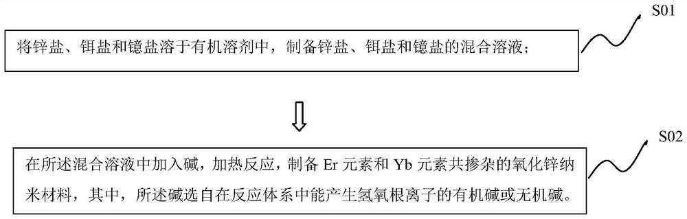
[0033] Correspondingly, combine figure 1 , The second aspect of the embodiment of the present invention provides a method for preparing a nanomaterial, comprising the following steps:

[0034] S01. Dissolving zinc salt, erbium salt and ytterbium salt in an organic solvent to prepare a mixed solution of zinc salt, erbium salt and ytterbium salt;

[0035] S02. adding alkali in the mixed solution, heating and reacting to prepare zinc oxide nanomaterials co-doped with Er elements and Yb elements, wherein the alkali is selected from organic bases or organic bases that can generate hydroxide ions in the reaction system Inorganic base.

[0036] The preparation method of the nanomaterial provided in the embodiment of the present invention only needs to dissolve zinc salt, erbium salt and ytterbium salt in an organic solvent, and then add alkali to react. The method is simple to operate and easy to realize large-scale preparation. More importantly, the nanomaterials prepared by the ...

Embodiment 1

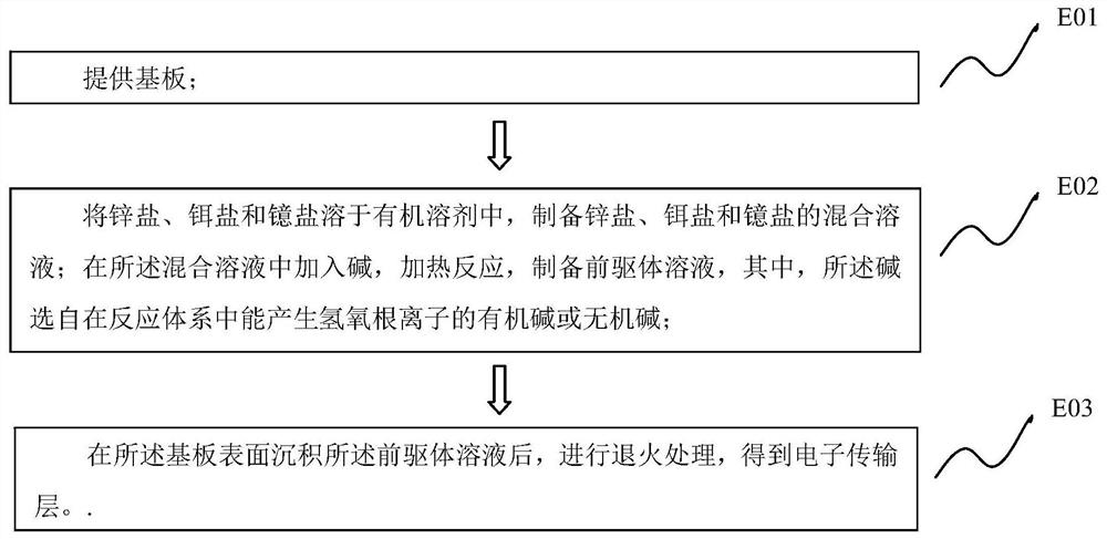
[0083] A method for preparing an electron transport thin film, comprising the following steps:

[0084] Add an appropriate amount of zinc sulfate, erbium sulfate and ytterbium sulfate into 50ml of ethanol, stir and dissolve at a temperature of 70°C to form a mixed solution with a total concentration of metal ions of 1mol / L. In the mixed solution, zinc ions and doped The molar ratio of ions (erbium ions and ytterbium ions) is 1:0.1, and the molar ratio of erbium ions and ytterbium ions is 2:1;

[0085] According to the molar ratio of hydroxide ions and metal ions of 1.8:1, an ethanol solution of potassium hydroxide was added to the mixed solution, and stirred at a temperature of 70°C for 4 hours to obtain a uniform transparent solution: Er -Yb / ZnO (Er-Yb / ZnO represents Er, Yb co-doped ZnO nanomaterial) solution;

[0086] After depositing the Er-Yb / ZnO solution on the surface of the substrate, annealing is performed at a temperature of 200° C. to obtain an electron transport th...

Embodiment 2

[0088] A method for preparing nanomaterials, comprising the steps of:

[0089] An appropriate amount of zinc nitrate, erbium nitrate and ytterbium nitrate are added in 50ml methanol, stirred and dissolved at 60°C, forming a mixed solution with a total concentration of metal ions of 1mol / L, in the mixed solution, zinc ions and dopant ions ( The molar ratio of erbium ion and ytterbium ion) is 1:0.15, and the molar ratio of erbium ion and ytterbium ion is 2.5:1;

[0090] According to the molar ratio of hydroxide ions and metal ions at a ratio of 2:1, a methanol solution of sodium hydroxide was added to the mixed solution, and stirred at a temperature of 60°C for 3 hours to obtain a uniform transparent solution: Er -Yb / ZnO (Er-Yb / ZnO represents Er, Yb co-doped ZnO nanomaterial) solution;

[0091] After depositing the Er-Yb / ZnO solution on the surface of the substrate, annealing is performed at a temperature of 150° C. to obtain an electron transport thin film.


PUM

PropertyMeasurementUnit
thicknessaaaaaaaaaa
thicknessaaaaaaaaaa

Abstract

The invention provides a nano material. The nano material comprises a ZnO nano material and doping elements doped in ZnO crystal lattices, and the doping elements are an Er element and a Yb element. According to the nano material provided by the invention, through co-doping of the Er element and the Yb element, the electron transmission capability of the ZnO nanometer material is improved, and when the ZnO nano material is used as an electron transmission layer of a quantum dot light-emitting diode, effective compounding of electrons and holes in a quantum dot light-emitting layer can be promoted, so that the influence of exciton accumulation on the performance of a device is reduced, and the light-emitting efficiency of the quantum dot light-emitting device is improved.

Description

technical field [0001] The invention belongs to the field of display technology, and in particular relates to a nanometer material and a preparation method thereof, as well as a quantum dot light-emitting diode and a preparation method thereof. Background technique [0002] Semiconductor quantum dots have a quantum size effect. People can adjust the size of quantum dots to achieve the required specific wavelength of light. For example, the luminescence wavelength of CdSe QDs can be tuned from blue light to red light. In traditional inorganic electroluminescent devices, electrons and holes are injected from the cathode and anode respectively, and then recombine in the light-emitting layer to form excitons to emit light. In recent years, the use of inorganic semiconductors as electron transport layers has become a relatively hot research topic. Nano-ZnO and ZnS are wide-bandgap semiconductor materials, which have attracted the attention of many researchers due to their advant...

Claims


Application Information

Patent Timeline
Patent Type & Authority Applications(China)
IPC IPC(8): C01G9/02B82Y20/00B82Y40/00H01L51/50
CPCC01G9/02B82Y20/00B82Y40/00H10K50/115H10K50/00
Inventor 何斯纳吴龙佳吴劲衡
Owner TCL CORPORATION
Why Eureka
Try Eureka