Electron transport material and preparation method thereof, photoelectric device and preparation method thereof

A technology for electron transport materials and optoelectronic devices, applied in the field of materials, can solve problems such as narrow band gaps, achieve the effects of reducing the impact of device performance, improving luminous efficiency, and increasing carrier concentration

Pending Publication Date: 2022-04-12
TCL CORPORATION
View PDF0 Cites 0 Cited by
  • Summary
  • Abstract
  • Description
  • Claims
  • Application Information

AI Technical Summary

Problems solved by technology

[0005] The purpose of this application is to provide an electron transport material and its preparation method, as well as a kind of optoelectronic device and its preparation method, aiming to solve the problem of existing TiS 2 There is a narrow band gap, which limits its application in optoelectronic devices

Method used


Image

  • Electron transport material and preparation method thereof, photoelectric device and preparation method thereof
  • Electron transport material and preparation method thereof, photoelectric device and preparation method thereof
  • Electron transport material and preparation method thereof, photoelectric device and preparation method thereof

Examples


preparation example Construction

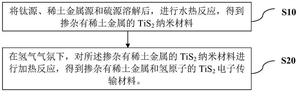
[0027] The first aspect of the embodiment of the present application provides a method for preparing an electron transport material, comprising the following steps:

[0028] S10. After dissolving titanium source, rare earth metal source and sulfur source, perform hydrothermal reaction to obtain TiS doped with rare earth metal 2 nanomaterials;

[0029] S20. In a hydrogen atmosphere, the TiS doped with rare earth metals 2 Nanomaterials undergo a heating reaction to obtain TiS doped with rare earth metals and hydrogen atoms 2 Electron transport materials.

[0030] The preparation method of the electron transport material provided by the first aspect of the present application comprises mixing and dissolving titanium source, rare earth metal source and sulfur source in water, and obtaining TiS doped with rare earth metal through hydrothermal reaction. 2 Nanomaterials; under hydrogen atmosphere, TiS doped with rare earth metals 2 Nanomaterial undergoes heating reaction to repla...

Embodiment 1

[0077] An electron transport material, comprising the following preparation steps:

[0078] ①First, add 1g of titanium sulfate and an appropriate amount of cerium sulfate into 50ml of water to form a solution with a total concentration of 0.5M, wherein the molar ratio of titanium: cerium is 1:0.1, and then add an appropriate amount of sodium sulfide (molar ratio, S 2- :M x+ =2.2:1). After being dispersed, it was transferred to a hydrothermal reaction tank, reacted at 200°C for 24 hours, and cooled and washed (washed twice with water and once with absolute ethanol). Then dried at 50 °C to obtain Ce / TiS 2 nanomaterials.

[0079] ②Add 1g Ce / TiS 2 The powder is spread on a boat-shaped crucible, placed in a muffle furnace and continuously fed with argon. After exhausting for 20 minutes, raise the temperature of the muffle furnace to 300°C, switch the argon gas to a hydrogen-containing argon mixed gas (5% hydrogen + 95% argon), keep the flow rate of the mixed gas at 80-100ml / mi...

Embodiment 2

[0081] An electron transport material, comprising the following preparation steps:

[0082] ①First, add 1g of titanium nitrate and appropriate amount of terbium nitrate into 50ml of water to form a solution with a total concentration of 0.5M, wherein the molar ratio of titanium: terbium is 1:0.2, and then add an appropriate amount of potassium sulfide (molar ratio, S 2- :M x+ =2.5:1). After being dispersed, it was transferred to a hydrothermal reaction kettle, reacted at 220°C for 24 hours, and cooled and washed (washed twice with water and once with absolute ethanol). Then dried at 50 °C to obtain Tb / TiS 2 nanomaterials.

[0083] ② Add 1g Tb / TiS 2 The powder is spread on a boat-shaped crucible, placed in a muffle furnace and continuously fed with argon. After exhausting for 20 minutes, raise the temperature of the muffle furnace to 300°C, switch the argon gas to a hydrogen-nitrogen mixed gas (8% hydrogen + 92% nitrogen), keep the flow rate of the mixed gas at 60-80ml / min...


PUM

PropertyMeasurementUnit
particle diameteraaaaaaaaaa
electrical conductivityaaaaaaaaaa

Abstract

The invention belongs to the technical field of materials, and particularly relates to a preparation method of an electron transport material, which comprises the following steps: dissolving a titanium source, a rare earth metal source and a sulfur source, and carrying out hydrothermal reaction to obtain a rare earth metal doped TiS2 nano material; and under a hydrogen atmosphere, carrying out a heating reaction on the TiS2 nano material doped with the rare earth metal to obtain the TiS2 electron transport material doped with the rare earth metal and hydrogen atoms. The preparation method of the electron transport material is simple in process and suitable for industrial large-scale production and application, and the prepared rare earth metal and hydrogen atom double-doped TiS2 electron transport material can effectively adjust the forbidden band width and the conductivity of the TiS2 material through synergistic co-doping of the rare earth metal and the hydrogen atoms, so that the electron transport material is suitable for large-scale production and application. The TiS2 material doped with rare earth metal and hydrogen atoms has better n-type semiconductor characteristics, and is more suitable for electron transport materials of photoelectric devices.

Description

technical field [0001] The application belongs to the technical field of materials, and in particular relates to an electron transport material and a preparation method thereof, and an optoelectronic device and a preparation method thereof. Background technique [0002] Semiconductor quantum dots have a quantum size effect. People can adjust the size of quantum dots to achieve the required specific wavelength of light. The emission wavelength of CdSe QDs can be tuned from blue light to red light. In traditional inorganic electroluminescent devices, electrons and holes are injected from the cathode and anode respectively, and then recombine in the light-emitting layer to form excitons to emit light. In recent years, the use of inorganic semiconductors as electron transport layers has become a relatively hot research topic. [0003] Nano ZnO, ZnS, TiO 2 , SnO 2 It has unique optical, electrical and physical properties, excellent chemical stability, and can resist electroche...

Claims


Application Information

Patent Timeline
Patent Type & Authority Applications(China)
IPC IPC(8): H01L51/54H01L51/50H01L51/56B82Y30/00
Inventor 何斯纳吴龙佳吴劲衡
Owner TCL CORPORATION
Why Eureka
Try Eureka