
Photoelectric artificial synapse preparation method and photoelectric artificial synapse

An artificial and synaptic technology, applied in photovoltaic power generation, circuits, electrical components, etc., can solve the problems of transmission barriers and the proportion of transmission power consumption cannot be ignored, and achieve fast response to light stimulation, good retention characteristics, and low energy consumption. Effect

Pending Publication Date: 2021-07-23
GUANGHUA LINGANG ENG APPL & TECH R&D (SHANGHAI) CO LTD
View PDF9 Cites 2 Cited by
  • Summary
  • Abstract
  • Description
  • Claims
  • Application Information

AI Technical Summary

Problems solved by technology

As one of the branches of artificial intelligence, machine vision and image recognition are developing rapidly, and have great application potential in industry, agriculture, transportation and other fields, but there are transmission barriers caused by the separation of information acquisition, data processing and storage
At present, the data processing capability (CPU) and data memory have reached a very high level, but the internal transmission delay has gradually become the biggest constraint, and the proportion of transmission power consumption cannot be ignored.

Method used


Image

  • Photoelectric artificial synapse preparation method and photoelectric artificial synapse
  • Photoelectric artificial synapse preparation method and photoelectric artificial synapse
  • Photoelectric artificial synapse preparation method and photoelectric artificial synapse

Examples


Embodiment Construction

[0021] The preparation method of the photoelectric artificial synapse and the specific implementation of the photoelectric artificial synapse provided by the present invention will be described in detail below in conjunction with the accompanying drawings.

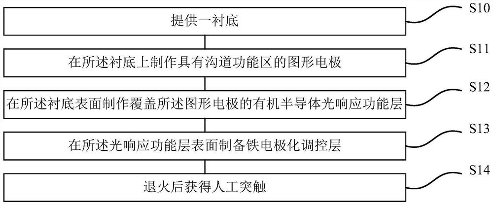
[0022] attached figure 1 Shown is a schematic diagram of the implementation steps of this specific embodiment, including: step S10, providing a substrate; step S11, making a patterned electrode with a channel functional area on the substrate; step S12, forming a substrate on the surface of the substrate Fabricating an organic semiconductor photoresponsive functional layer covering the patterned electrodes; step S13, preparing a ferroelectric polarization regulation layer on the surface of the photoresponsive functional layer; step S14, obtaining an artificial synapse after annealing.

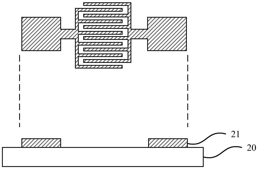
[0023] attached Figure 2A As shown, referring to step S10, a substrate 20 is provided. The substrate 20 is selected from one of silicon,...


PUM

PropertyMeasurementUnit
Thicknessaaaaaaaaaa

Abstract

The invention provides a photoelectric artificial synapse preparation method. The preparation method comprises the following steps: providing a substrate; manufacturing a pattern electrode with a channel functional region on the substrate; manufacturing an organic semiconductor photoresponse function layer covering the pattern electrode on the surface of the substrate; preparing a ferroelectric polarization regulation and control layer on the surface of the photoresponse functional layer; and annealing to obtain the artificial synapse. Implementation of the artificial synapse is based on ferroelectric polarization multi-stage regulation and photoelectric response of an organic photoelectric semiconductor. And a high-quality in-plane polarization ferroelectric film is obtained by using a dispensing method to construct a planar multilayer structure. Compared with other memristor artificial synapses depending on conductive filaments and ion doping, the artificial synapses has the advantages of low operation voltage, good retention characteristic, simple and controllable preparation process and the like. The method can simulate important synaptic functions, is fast in response to photostimulation and low in energy consumption, and can be used in the fields of neuromorphic calculation, image recognition, machine vision, convolutional neural networks and the like.

Description

technical field [0001] The invention relates to the field of semiconductor devices, in particular to a preparation method of a photoelectric artificial synapse and a photoelectric artificial synapse. Background technique [0002] With the rapid development of electronic information technology, artificial intelligence, as one of the three cutting-edge technologies in the 21st century, has achieved subversive development in just a few decades. As one of the branches of artificial intelligence, machine vision and image recognition are developing rapidly, and have great application potential in industry, agriculture, transportation and other fields, but there are transmission barriers caused by the separation of information acquisition, data processing and storage. At present, the data processing capability (CPU) and data memory have reached a very high level, but the internal transmission delay has gradually become the biggest constraint, and the proportion of transmission powe...

Claims


Application Information

Patent Timeline
IPC IPC(8): H01L51/48H01L51/42H01L51/44G06N3/04
CPCG06N3/045H10K71/12H10K71/40H10K71/60H10K30/20H10K30/81Y02E10/549Y02P70/50
Inventor 胡来归蔡依辰詹义强秦亚杰
Owner GUANGHUA LINGANG ENG APPL & TECH R&D (SHANGHAI) CO LTD
Learn More