Single-layer fluorinated graphene Schottky diode and preparation method and application thereof

A Schottky diode and single-layer graphene technology, which is applied in semiconductor/solid-state device manufacturing, electrical components, circuits, etc., can solve the problem of difficult adjustment of Schottky diode performance parameters, short reverse recovery time, and device performance degradation, etc. question

Active Publication Date: 2021-07-30
TSINGHUA UNIV
View PDF5 Cites 3 Cited by
  • Summary
  • Abstract
  • Description
  • Claims
  • Application Information

AI Technical Summary

Problems solved by technology

However, the size of the graphene Schottky diode processed by S.Kim et al. is basically determined by its substrate, resulting in the thickness of the device being much larger than nanometers; The Schottky barrier height of the Tertky junction is completely determined by the material of the semiconductor itself, which makes it difficult to adjust the performance parameters of the manufactured Schottky diode due to the limited range of semiconductor material selection; and the impurities and defects of the semiconductor substrate will This leads to a decrease in device performance, and it is impossible to realize a real high-performance nano-Schottky diode device
[0005] In summary, graphene Schottky diodes have the advantages of reduced forward voltage and short reverse recovery time, but existing methods only use graphene as a Half-metals and semiconductors contact to form Schottky junctions, the size of which is much larger than the nanometer scale, which cannot fully reflect the advantages of graphene two-dimensional materials, and the device performance is easily affected by substrate impurities and defects

Method used


Image

  • Single-layer fluorinated graphene Schottky diode and preparation method and application thereof
  • Single-layer fluorinated graphene Schottky diode and preparation method and application thereof
  • Single-layer fluorinated graphene Schottky diode and preparation method and application thereof

Examples


Embodiment 1

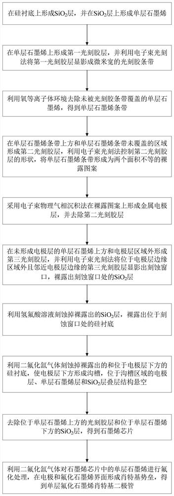
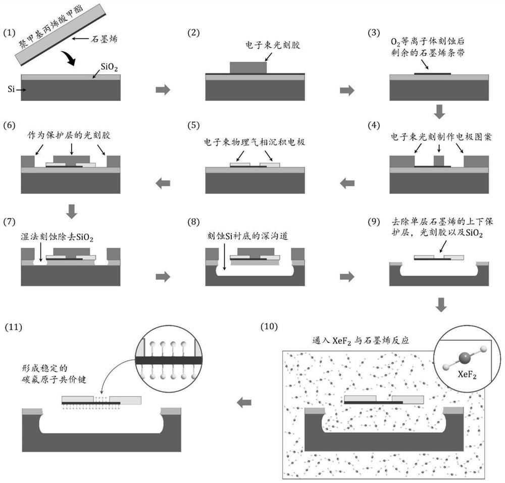
[0136] A preparation method of a novel monolayer fluorinated graphene Schottky diode. According to an embodiment of the invention:

[0137] (1) Firstly, it is necessary to prepare a graphene structure with a single-layer suspension, and the specific implementation is as follows:

[0138] (1-1) Single-layer graphene (SLG: Single-layer graphene) was prepared by chemical vapor deposition, and then transferred to a 100nm thick SiO 2 layer on a 4-inch Si wafer (as attached figure 2 (1)), and then cut it into chips with a size of 1cm×1cm for subsequent MEMS processing.

[0139] (1-2) Spin-coat a layer of electron beam photoresist (ZEP520A) with a thickness of 300nm on the surface of SLG, and use electron beam lithography to expose and develop the photoresist to form micron-wide photoresist strips (such as attached figure 2 shown in (2)).

[0140] (1-3) Expose the chip to O 2 (Oxygen) plasma for 30s, and etch away the SLG not covered by photoresist (as attached figure 2 sho...


PUM

PropertyMeasurementUnit
thicknessaaaaaaaaaa
thicknessaaaaaaaaaa
thicknessaaaaaaaaaa

Abstract

The invention discloses a single-layer fluorinated graphene Schottky diode and a preparation method and application thereof. According to the method, a composite etching process is adopted, a deep groove is formed in a silicon substrate, the whole single-layer graphene diode device is made to suspend on the groove, and meanwhile a metal electrode is prepared on the single-layer graphene diode device; moreover, the graphene is fluorinated through xenon difluoride (XeF2) gas, an electron energy band gap is opened, a stable fluorocarbon atom covalent bond is formed in a suspended part, and a Schottky barrier is formed on an interface of a metal electrode and the fluorinated graphene to trigger a diode effect. By adopting the method, the influence of the semiconductor substrate on the thickness of the Schottky diode device and the negative influence of doping / impurities or defects of the semiconductor substrate on the performance of the Schottky diode device can be avoided, and the Schottky diode has the advantages of high response frequency, high electron migration rate and the like; and the method is of great significance to the development of integrated circuits under the micro-nano scale.

Description

technical field [0001] The invention belongs to the field of two-dimensional nanomaterial electronic devices, in particular, it relates to a Schottky diode of single-layer fluorinated graphene, a preparation method and application thereof. Background technique [0002] Schottky diodes are also called Schottky barrier diodes (SBD: Schottky Barrier Diode). The principle is that the concentration of free electrons on both sides of the metal and semiconductor contact interface is not equal, so that electron diffusion forms a Schottky barrier to form a diode rectification effect. SBDs have many advantages over classic PN junction diodes. First of all, because the Schottky barrier height is generally lower than the PN junction barrier, the Schottky diode has a lower forward conduction voltage, which is about 150mV-450mV, and the corresponding PN junction diode is about 600mV-700mV. The low-voltage drop characteristics of Schottky diodes are often used as low-cost photovoltaic cel...

Claims


Application Information

Patent Timeline
Patent Type & Authority Applications(China)
IPC IPC(8): H01L21/329H01L21/28H01L21/04H01L29/06H01L29/16H01L29/167H01L29/47H01L29/872
CPCH01L29/6603H01L29/872H01L29/0684H01L29/1606H01L29/167H01L21/0435H01L29/47Y02P70/50
Inventor 王海东朱虹鑫谢思齐赵帅伊周要洪
Owner TSINGHUA UNIV
Why Eureka
Try Eureka