Low-power-consumption flexible thin film transistor based on three layers of insulating media and manufacturing method of low-power-consumption flexible thin film transistor

A flexible film and three-layer insulation technology, which is applied in the manufacture of semiconductor/solid-state devices, electric solid-state devices, semiconductor devices, etc., can solve the limitations of the practical application of flexible organic field effect transistors, large energy consumption, and does not meet the development trend of low energy consumption, etc. question

Pending Publication Date: 2021-08-24
XIDIAN UNIV +2
View PDF9 Cites 0 Cited by
  • Summary
  • Abstract
  • Description
  • Claims
  • Application Information

AI Technical Summary

Problems solved by technology

[0005]For example, the carrier mobility of organic field-effect transistors based on flexible substrates is mostly significantly lower than that of rigid organic transistors based on silicon, which will Limiting the Practical Applications of Flexible Organic Field-Effect Transistors
[0006]For example, the operating voltage of traditional organic field effect transistor devices is relatively high, resulting in large energy consumption, which does not meet the current development trend of low energy consumption and portability

Method used


Image

  • Low-power-consumption flexible thin film transistor based on three layers of insulating media and manufacturing method of low-power-consumption flexible thin film transistor
  • Low-power-consumption flexible thin film transistor based on three layers of insulating media and manufacturing method of low-power-consumption flexible thin film transistor
  • Low-power-consumption flexible thin film transistor based on three layers of insulating media and manufacturing method of low-power-consumption flexible thin film transistor

Examples


Embodiment Construction

[0046] Below in conjunction with accompanying drawing, further describe the present invention in detail through embodiment.

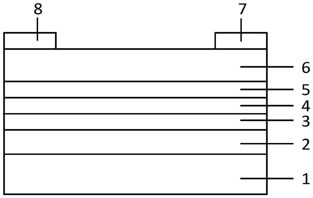
[0047] Such as figure 1 Shown is a specific implementation structure of a low-power flexible thin film transistor based on a three-layer insulating medium, including:

[0048] A flexible substrate 1 made of polyethylene terephthalate (Poly (ethylene Terephthalate), PET); of course, PDMS (polydimethylsiloxane), PI (polyimide) can also be used according to actual needs. ) or PEN (polyethylene naphthalate) and other materials;

[0049] The aluminum (Aluminium, Al) gate electrode 2 located on the upper surface of the PET flexible substrate; of course, it can also be made of metal materials such as gold or silver according to actual needs;

[0050] Aluminum oxide (Aluminum Oxide, Al 2 o 3 ) insulating gate dielectric film 3;

[0051] A polymethyl methacrylate (Poly(MethylMethacrylate), PMMA) insulating dielectric film 4 located on the upper surface of t...


PUM

PropertyMeasurementUnit
Thicknessaaaaaaaaaa
Deposition thicknessaaaaaaaaaa
Thicknessaaaaaaaaaa

Abstract

The invention discloses a low-power-consumption flexible thin film transistor based on three layers of insulating media and a manufacturing method of the low-power-consumption flexible thin film transistor. The low-power-consumption flexible thin film transistor adopts a bottom gate top contact structure and is sequentially composed of a flexible substrate, a gate electrode, an insulating dielectric layer, an active layer, a source electrode and a drain electrode. According to the invention, Al2O3 with a high dielectric constant is adopted as an inorganic material insulating dielectric layer, the working voltage and the threshold voltage can be effectively reduced, but high interface polarity is brought about by the high dielectric constant; and in order to reduce the interface polarity, an insulating medium film made of PMMA and a cross-linked PVP-HDA insulating medium film obtained by mixing a cross-linking agent 4, 4 '-(hexafluoroisopropenyl) diphthalic anhydride and poly (4-vinylphenol) are added. The flexible thin film transistor can well balance the contradiction between the dielectric constant and the interface polarity, has the advantages of being low in power consumption, small in leakage current, low in subthreshold swing and the like, is simple in process and low in cost, and facilitates large-scale production.

Description

technical field [0001] The invention relates to the field of flexible electronic systems, in particular to a low power consumption flexible organic thin film transistor based on a three-layer insulating medium and a manufacturing method thereof. Background technique [0002] The device density in integrated circuits is growing steadily in accordance with the famous Moore's Law in the semiconductor industry, basically achieving the goal of doubling every 18 months, and the precision of semiconductor processes has also increased. However, the research on traditional inorganic semiconductor materials is close to its physical limit, and it will be extremely difficult to continue to reduce the feature size of devices due to adverse factors such as short channel effects and quantum tunneling effects. Therefore, flexible organic semiconductor materials and devices with simple process and low cost have been discovered and gradually become a new research hotspot. [0003] Transistor...

Claims


Application Information

Patent Timeline
IPC IPC(8): H01L51/05H01L51/10H01L51/40
CPCH10K71/12H10K10/476H10K10/466H10K77/111Y02E10/549Y02P70/50
Inventor 段宝兴唐春萍孙佳刘婉蓉杨银堂
Owner XIDIAN UNIV
Why Eureka
Try Eureka