

Method for growing thin-layer high-resistance silicon epitaxial wafer and prepared epitaxial wafer
A technology for epitaxial wafers and high-resistance silicon, applied in crystal growth, single crystal growth, single crystal growth, etc., can solve problems such as increased epitaxy costs, surface quality of epitaxy defects, and increased influence of system self-doping, so as to suppress impurity diffusion and evaporation, reducing solid-state diffusion and gas-phase self-doping, and reducing the effect of system self-doping
- Summary
- Abstract
- Description
- Claims
- Application Information
AI Technical Summary
Problems solved by technology
Method used
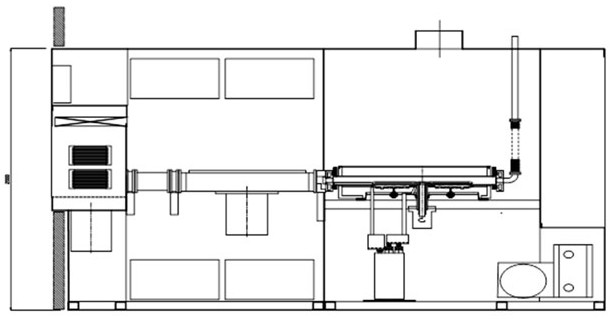
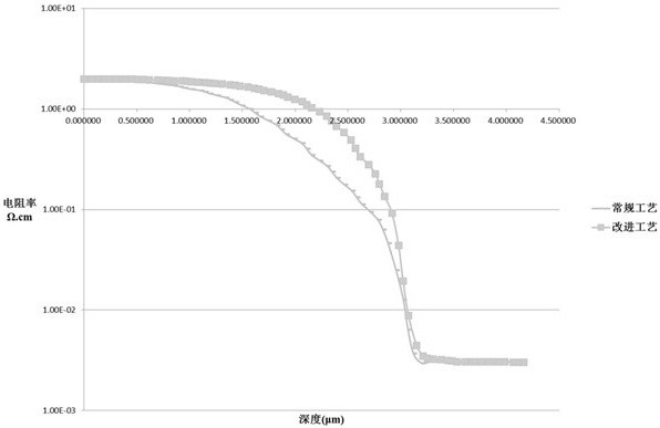
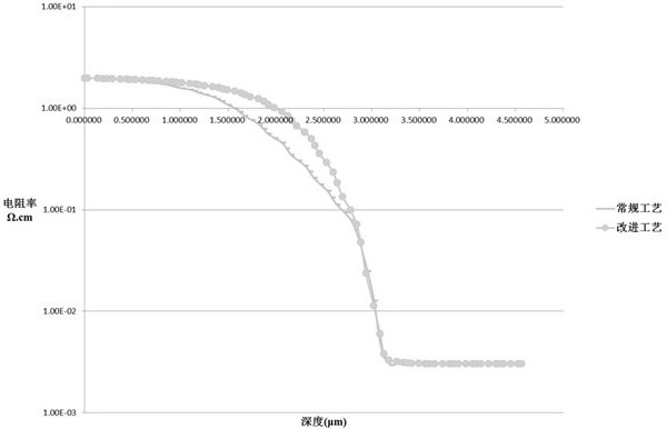
Image

Examples
Embodiment 1
[0027] A method for growing a thin-layer high-resistance silicon epitaxial wafer on a heavily doped As substrate, comprising the following steps:
[0028] (1) Use high-flow HCL to clean the reaction chamber and graphite base before loading to remove reaction residues.
[0029] (2) As-doped substrate is selected, and the resistivity is 0.001~0.004Ω.cm; the back of the substrate is sealed with silicon dioxide, and the edge width of the back-sealing layer is only removed from the chamfered surface.
[0030] (3) To grow the first epitaxial layer, set the pressure of the reaction chamber to 30Torr, grow the first epitaxial layer on the surface of the substrate with a growth temperature of 1080°C and a growth rate of 0.7 μm / min, and the first epitaxial layer cannot pass dopants gas. A pure epitaxial layer is grown on the surface of the substrate with a low growth temperature and a low growth rate, and the growth temperature, growth rate and epitaxy time are controlled to effectivel...
Embodiment 2
[0036] A method for growing a thin-layer high-resistance silicon epitaxial wafer on a heavily doped As substrate, comprising the following steps:
[0037] (1) Use high-flow HCL to clean the reaction chamber and graphite base before loading to remove reaction residues.
[0038] (2) As-doped substrate is selected, and the resistivity is 0.001~0.004Ω.cm; the back of the substrate is sealed with silicon dioxide, and the edge width of the back-sealing layer is only removed from the chamfered surface.
[0039] (3) Carry out the growth of the first epitaxial layer, set the pressure of the reaction chamber to 10Torr, grow the first epitaxial layer on the substrate surface with a growth temperature of 1050°C, and a growth rate of 0.5 μm / min, and the first epitaxial layer cannot pass dopants gas. A pure epitaxial layer is grown on the surface of the substrate with a low growth temperature and a low growth rate, and the growth temperature, growth rate and epitaxy time are controlled to ...
Embodiment 3
[0045] A method for growing a thin-layer high-resistance silicon epitaxial wafer on a heavily doped As substrate, comprising the following steps:
[0046] (1) Use high-flow HCL to clean the reaction chamber and graphite base before loading to remove reaction residues.
[0047] (2) As-doped substrate is selected, and the resistivity is 0.001~0.004Ω.cm; the back of the substrate is sealed with silicon dioxide, and the edge width of the back-sealing layer is only removed from the chamfered surface.
[0048](3) To grow the first epitaxial layer, set the pressure of the reaction chamber to 50Torr, grow the first epitaxial layer on the substrate surface with a growth temperature of 1100°C, and a growth rate of 1.0 μm / min, and the first epitaxial layer cannot pass dopants gas. A pure epitaxial layer is grown on the surface of the substrate with a low growth temperature and a low growth rate, and the growth temperature, growth rate and epitaxy time are controlled to effectively encap...
PUM
| Property | Measurement | Unit |
|---|---|---|
| electrical resistivity | aaaaa | aaaaa |
| evenness | aaaaa | aaaaa |
| evenness | aaaaa | aaaaa |
Abstract
Description
Claims
Application Information