Porous GaN narrow-band ultraviolet photodiode and preparation method thereof
A technology of ultraviolet light and diodes, applied in circuits, electrical components, semiconductor devices, etc., to achieve the effects of improving light absorption, high conductivity, and reducing material defects
- Summary
- Abstract
- Description
- Claims
- Application Information
AI Technical Summary
Problems solved by technology
Method used
Image
Examples
Embodiment 1
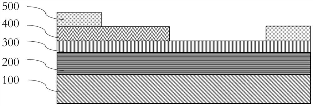
[0047] Such as figure 1 and 2 As shown, this embodiment provides a porous GaN narrowband ultraviolet photodiode, including a substrate layer 100, a semiconductor layer 200, a porous GaN layer 300, a CuZnS layer 400, and a metal contact layer 500. In this embodiment, the substrate layer 100 is a sapphire substrate layer, and the semiconductor layer 200 is arranged on the upper surface of the substrate layer 100. In this embodiment, the semiconductor layer 200 is a GaN thin film layer; and the carrier of the GaN thin film layer at room temperature The concentration range is 1×10 15 to 1×10 18 cm -3 , with a thickness of 4-6 μm. The semiconductor layer 200 is provided with a porous GaN layer 300 and a CuZnS layer 400 , and the upper surfaces of the porous GaN layer 300 and the CuZnS layer 400 are provided with a metal contact layer 500 . The CuZnS layer 400 described in this embodiment has a thickness of 30-100 nm. The metal contact layer 500 is an ohmic contact layer, and ...
Embodiment 2
[0049] This embodiment provides a method for preparing a porous GaN narrow-band ultraviolet photodiode, the method comprising:
[0050] S1), depositing a GaN thin film on the substrate layer 100, wherein the thickness of the deposited GaN thin film is 5000nm;
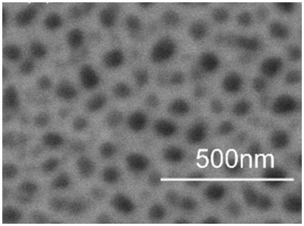
[0051] S2), cleaning the GaN film prepared in step S1), and etching a part of the GaN film with an ionic liquid to form a porous GaN layer 300;
[0052] S3), another part of the GaN thin film is used to form a CuZnS layer 400 on the surface with a water bath method, wherein the Cu component is 20%.
[0053] As preferred in this embodiment, in step S2), before etching the porous GaN layer 300, put GaN of 1.0 cm×0.3 cm in aqua regia to remove the passivation layer on the surface, take it out after five minutes; then use acetone, Ultrasonic cleaning of the GaN sheet in ethanol and deionized water, 30 minutes each time; followed by a hydrophilic treatment of the GaN sheet in an ultraviolet ozone cleaner to enhance the cont...
Embodiment 3
[0060] This embodiment provides a method for preparing a porous GaN narrow-band ultraviolet photodiode, the method comprising:
[0061] S1), depositing a GaN thin film on the substrate layer 100, wherein the thickness of the deposited GaN thin film is 5000nm;
[0062] S2), cleaning the GaN film prepared in step S1), and etching a part of the GaN film with an ionic liquid to form a porous GaN layer 300;
[0063] S3), another part of the GaN thin film is used to form a CuZnS layer 400 on the surface with a water bath method, wherein the Cu component is 10%.
[0064] As preferred in this embodiment, in step S2), before etching the porous GaN layer 300, put GaN of 1.0 cm×0.3 cm in aqua regia to remove the passivation layer on the surface, take it out after five minutes; then use acetone, Ultrasonic cleaning of the GaN sheet in ethanol and deionized water, 30 minutes each time; followed by a hydrophilic treatment of the GaN sheet in an ultraviolet ozone cleaner to enhance the cont...
PUM
| Property | Measurement | Unit |
|---|---|---|
| Carrier concentration | aaaaa | aaaaa |
| Thickness | aaaaa | aaaaa |
| Thickness | aaaaa | aaaaa |
Abstract
Description
Claims
Application Information
 - R&D
- Intellectual Property
- Life Sciences
- Materials
- Tech Scout
- Unparalleled Data Quality
- Higher Quality Content
- 60% Fewer Hallucinations
Browse by: Latest US Patents, China's latest patents, Technical Efficacy Thesaurus, Application Domain, Technology Topic, Popular Technical Reports.
© 2025 PatSnap. All rights reserved.Legal|Privacy policy|Modern Slavery Act Transparency Statement|Sitemap|About US| Contact US: help@patsnap.com


