Preparation method of selective emitter of crystalline silicon solar cell

A solar cell and selective technology, applied in the direction of circuits, photovoltaic power generation, electrical components, etc., can solve problems that are not conducive to increasing short-circuit current, increasing equipment operating costs, and increasing open-circuit voltage, so as to improve photoelectric conversion efficiency and facilitate industrial use , The effect of improving the conversion efficiency

Pending Publication Date: 2022-01-07
HUNAN RED SUN PHOTOELECTRICITY SCI & TECH
View PDF0 Cites 0 Cited by
  • Summary
  • Abstract
  • Description
  • Claims
  • Application Information

AI Technical Summary

Problems solved by technology

Conventional boron diffusion uses boron tribromide or boron trichloride, both process gases will cause corrosion to the quartz parts; long-term operation will cause damage to the quartz parts and increase the operating cost of the equipment
In addition, with boron diffusion, the doping concentration of the surface borosilicate glass is only 1E 19 atoms / cm 3 Due to the low doping concentration, it is difficult to form a selective emitter, or it is difficult to reduce the contact resistance and metal recombination in the heavily doped region, which is not conducive to improving the open circuit voltage; at the same time, due to the low doping concentration, it cannot effectively improve The Auger recombination and short-wave quantum efficiency in the lightly doped region are not conducive to improving its short-circuit current, so that the effect of the selective emitter on improving the conversion efficiency of solar cells is not obvious

Method used


Image

  • Preparation method of selective emitter of crystalline silicon solar cell
  • Preparation method of selective emitter of crystalline silicon solar cell
  • Preparation method of selective emitter of crystalline silicon solar cell

Examples


Embodiment 1

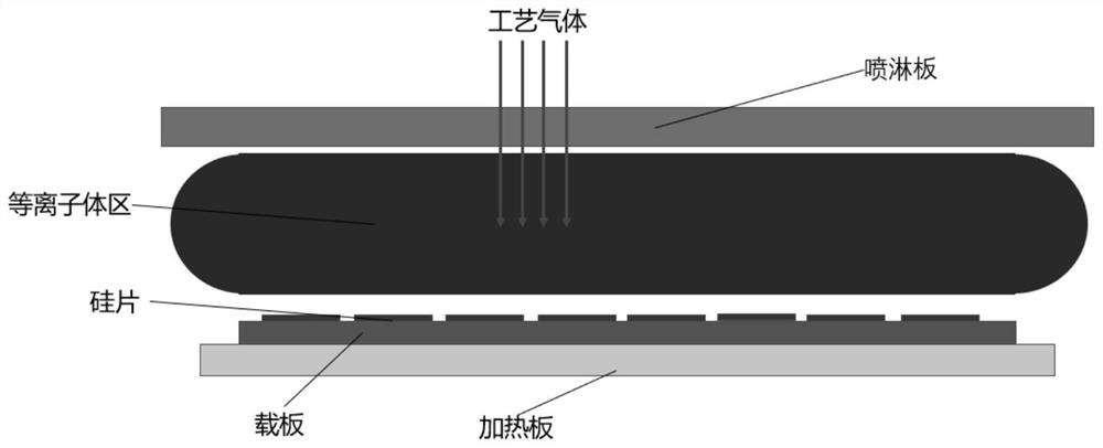
[0032] A method for preparing a selective emitter of a crystalline silicon solar cell. The selective emitter is prepared by borosilicate glass deposition, laser selective localized doping and high-temperature push junction technology, and the PECVD equipment and high-temperature annealing furnace used are Hunan Red Sunlight Technology Co., Ltd. PECVD equipment (such as figure 1 Shown) and high temperature annealing furnace, laser equipment is Wuhan Dier laser equipment, including the following steps:

[0033] (1) Prepare the doping concentration of boron atoms on the surface of the silicon substrate to be 1.3E 21 atoms / cm 3 The borosilicate glass film:

[0034](1.1) Place the carrier plate carrying the silicon substrate (n-type silicon wafer) in the reaction device (PECVD equipment), evacuate it to below 0.05mbar, and heat the reaction chamber (process chamber) until the temperature is 400°C, where the distance between parallel plates in the PECVD equipment (the distance be...


PUM


Abstract

The invention discloses a preparation method of a selective emitter of a crystalline silicon solar cell. The preparation method comprises the following steps of preparing a borosilicate glass film of which the boron atom doping concentration is greater than or equal to 1E21 atoms/cm <3> on the surface of a silicon substrate; carrying out local doping on the borosilicate glass film in the metal contact area on the surface of the silicon substrate by adopting laser; and performing high-temperature annealing on the locally doped silicon substrate to complete the preparation of the selective emitter of the crystalline silicon solar cell. According to the preparation method disclosed by the invention, the borosilicate glass film with high doping concentration is prepared on the surface of the silicon substrate, and then the selective emitter of the crystalline silicon solar cell with better performance is prepared through laser selective doping and high-temperature annealing treatment, so that the photoelectric conversion efficiency of the crystalline silicon solar cell is remarkably improved; meanwhile, the preparation method also has the advantages of simple process, convenience in operation, easiness in control and the like, can be used for preparing by directly utilizing an existing device, and is high in suitability and is convenient for industrial utilization.

Description

technical field [0001] The invention belongs to the field of solar cells, and relates to a method for preparing a selective emitter of a crystalline silicon solar cell. Background technique [0002] Boron diffusion is widely used in the field of solar cells. In the preparation of high-efficiency cells such as Tunneling Oxide Passivated Contact (TOPCon) cells and Passivated Emitter Back Local Diffusion (PERL) cells, boron diffusion needs to be carried out on the front surface of silicon wafers. Boron diffusion creates a p-n junction. Conventional boron diffusion uses boron tribromide or boron trichloride, both of which will corrode the quartz parts; long-term operation will cause damage to the quartz parts and increase the operating cost of the equipment. In addition, with boron diffusion, the doping concentration of the surface borosilicate glass is only 1E 19 atoms / cm 3 Due to the low doping concentration, it is difficult to form a selective emitter, or it is difficult ...

Claims


Application Information

Patent Timeline
Patent Type & Authority Applications(China)
IPC IPC(8): H01L31/0224H01L31/068H01L31/18
CPCH01L31/022425H01L31/068H01L31/1804Y02E10/547
Inventor 许烁烁张威杨斌徐伟李涛吴易龙
Owner HUNAN RED SUN PHOTOELECTRICITY SCI & TECH
Why Eureka
Try Eureka