Optical waveguide amplifier and preparation method thereof

An optical waveguide amplifier and waveguide technology, which is applied in the field of optical communication, can solve the problems of lack of preparation methods for optical waveguide amplifiers, achieve the effects of improving gain and pumping efficiency, improving processing efficiency, and not being easily broken

Active Publication Date: 2022-01-14
HUAZHONG UNIV OF SCI & TECH
View PDF8 Cites 0 Cited by
  • Summary
  • Abstract
  • Description
  • Claims
  • Application Information

AI Technical Summary

Problems solved by technology

[0006] In summary, prior art still lacks a kind of production stable optical waveguide amplifier preparation method

Method used


Image

  • Optical waveguide amplifier and preparation method thereof
  • Optical waveguide amplifier and preparation method thereof
  • Optical waveguide amplifier and preparation method thereof

Examples


Embodiment 1

[0043] A optical waveguide escape device, such as Figure 1-8 As shown, it is prepared by the following method:

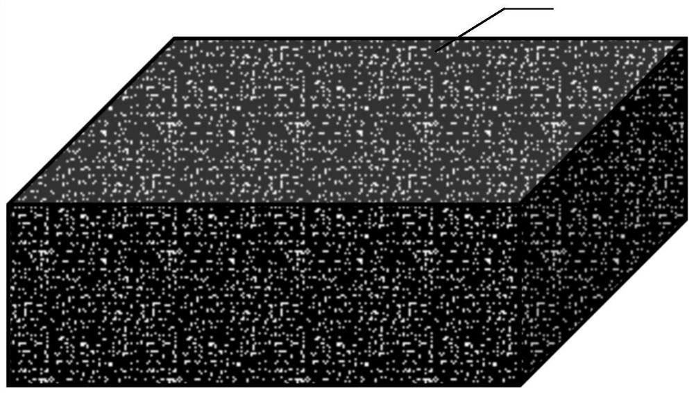
[0044]Step S1: Take a length of 2 cm, 2 cm, 1.5 mm, and the porous glass 1 has a three-dimensional contact nanoporous aperture structure, and the internal air hole is 0.4 nm; The porous glass is a quartz nanoporous glass prepared by thermogravime, specifically weighs 7 mol silica, 1.25 mol tetraborate, 0.5 mol sodium carbonate is placed in a crucible mixed, after melt, molding, annealing, and division After the phase and the acid treatment operation, rinse with deionized water, dried at 380 ° C to give quartz nanoporous glass after drying.

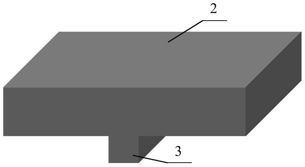
[0045] Step S2: Type T-type Application Template 2 is machined on a substrate made of silicon according to electron beam etching, and a T-shaped press mold plate 2 has a rectangular cuboid projection 3, and the long square projection 3 is long. 3 cm, 5 microns, 8 microns, respectively.

[0046] Step S3: The intermediate portion abov...


PUM

PropertyMeasurementUnit
diameteraaaaaaaaaa
widthaaaaaaaaaa
heightaaaaaaaaaa

Abstract

The invention belongs to the technical field of optical communication, and particularly relates to an optical waveguide amplifier and a preparation method thereof. The preparation method disclosed by the invention comprises the following steps: (1) processing a substrate to form a groove, wherein the substrate is porous glass with a three-dimensional communicated nanoscale pore channel structure; (2) transferring an erbium salt solution to the bottom of the groove, so that erbium ions are diffused into the porous glass to form an erbium-doped waveguide; and (3) depositing the erbium-doped waveguide to enable the erbium-doped waveguide to be sealed by a deposition material which is the same as the porous glass in material, and peforming sintering after deposition to obtain the optical waveguide amplifier. The doping concentration of Er < 3 + > is improved by utilizing the characteristics of the porous glass, the clustering effect of Er < 3 + > is inhibited, and the preparation stability of the optical waveguide amplifier is improved by utilizing a new method.

Description

Technical field [0001] The present invention belongs to the field of optical communication, and more particularly to a light waveguide array and a preparation method thereof. Background technique [0002] Signal light There is a certain loss and dispersion when transmitting in the fiber, which has seriously limited the transmission distance of the signal light. In order to ensure the transmission quality of the signal light, it is necessary to enhance the signal light, and the typical optical amplifier has a semiconductor optical amplifier, an optical fiber amplifier, and a light waveguide. The semiconductor optical amplifier is simple, the process matures, but the maximum weakness is too large, noise and crosstalk, noise and crosstalk and is susceptible to ambient temperature, so the stability is poor. The fiber amplifier has strong anti-interference ability, and the coupling loss is low, but the fiber amplifier is too long, which is not conducive to the miniaturization of the d...

Claims


Application Information

Patent Timeline
Patent Type & Authority Applications(China)
IPC IPC(8): G02F1/39
CPCG02F1/395
Inventor 杨旅云苏魏全马云秀
Owner HUAZHONG UNIV OF SCI & TECH
Why Eureka
Try Eureka