A Surface Treatment Method for Improving the Bonding Performance of Multilayer Plating Materials

A technology of surface treatment and multi-layer plating, which is applied in welding equipment, laser welding equipment, manufacturing tools, etc., can solve the problems of lack of laser surface treatment solutions, insufficient and other problems, and meet strength requirements, improve surface roughness, and meet air tightness requirements. The effect of sexual demands

Active Publication Date: 2022-04-08
广东华智芯电子科技有限公司
View PDF12 Cites 0 Cited by
  • Summary
  • Abstract
  • Description
  • Claims
  • Application Information

AI Technical Summary

Problems solved by technology

In the prior art, there are mainly technical solutions for laser surface treatment on a single alloy metal to improve bonding performance, but there is a lack of laser surface treatment solutions for multi-layer plating materials (semiconductors), that is, how to control laser parameters, One or more layers of coating required for arbitrary removal without affecting the underlying material
[0003] Although the use of existing technologies can also improve the bonding performance of semiconductors, for semiconductor packaging, the bonding performance is not enough to satisfy the package without breaking (the adhered parts meet the reliability verification and do not fall off), which is far from enough

Method used


Image

  • A Surface Treatment Method for Improving the Bonding Performance of Multilayer Plating Materials
  • A Surface Treatment Method for Improving the Bonding Performance of Multilayer Plating Materials
  • A Surface Treatment Method for Improving the Bonding Performance of Multilayer Plating Materials

Examples


Embodiment 1

[0049] 1. The processing equipment and materials involved in this embodiment

[0050] (1) The laser uses an IPG fiber laser, which emits a pulsed laser with a wavelength of 1064nm and a pulse width of 200ns (fixed and non-adjustable).

[0051] (2) The CPM material is a multi-layer composite material of copper, molybdenum-copper, and tungsten-copper core materials. It has high thermal conductivity, and the coefficient of thermal expansion (CTE) is easy to adjust. It is easy to match with Kovar alloy and alumina ceramics. It is currently the mainstream Heat dissipation substrate for high-power chips. CPC is a kind of CPM material. The default CPC core material in the industry refers to Mo70Cu30 material. Because copper (Cu) is easily oxidized and corroded in the air, which affects the life of CPC core material, nickel (Ni), Gold (Au) coats its surface to extend the lifetime of the CPC. In the field of electronic packaging, the connection between CPC and lead frame, its reliabili...

Embodiment approach 1

[0055] Using the first laser with power of 5W and frequency of 60KHz, and the second laser with power of 15W and frequency of 40KHz, the surface of the CPC multilayer coating material was treated according to the surface treatment method of the present invention to obtain sample one.

[0056] Using a laser with a power of 15W and a frequency of 40KHz, the surface of the CPC multilayer coating material was treated according to the surface treatment method in the prior art, and sample 2 was obtained.

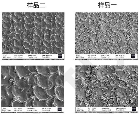
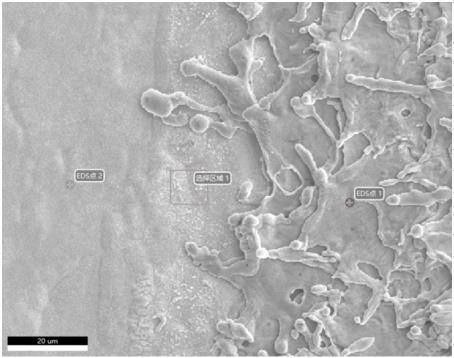
[0057] Sample 1 and sample 2 were tested for microstructure, bonding area strength and packaging airtightness respectively:

[0058] (1) Microstructure detection

[0059] see Figure 2-Figure 4 As shown, among them, figure 2 is the surface microscopic topography of sample 1 and sample 2; image 3 Sampling diagram for sample-surface EDS detection; Figure 4 It is the EDS detection spectrogram; Table 2 is the EDS detection quantitative result table.

[0060] During the bonding...

Embodiment approach 2

[0077] Adopting power is 5W, and the frequency is the first laser of 60KHz, and power is 15W, and the frequency is the second laser of 40KHz, according to the surface treatment method of the present invention, the surface of two CPC multilayer coating materials is processed respectively, obtains sample three And sample four, the difference is: the area layer in the step (S1) followed by sample three, where the line spacing between the filled lines is 0.03mm (less than 0.05mm); in the step (S1) followed by sample four Area layers where the line spacing between filled lines is 0.1mm (greater than 0.05mm).

[0078] refer to Image 6 and as shown in Table 4, Image 6 It is the optical photo of sample 3 and sample 4, and Table 4 is the comparison table of the results of sample 3 and sample 4. According to Embodiment 2, in the step (S1) of the present invention, the line spacing between the filling lines of the surface treatment area layer is less than 0.05mm, and the function is ...


PUM

PropertyMeasurementUnit
electrical resistivityaaaaaaaaaa
wavelengthaaaaaaaaaa

Abstract

The invention discloses a surface treatment method for improving the bonding performance of multi-layer plating materials, relates to the technical field of integrated circuit packaging, and includes setting a surface treatment area layer, a first laser with a power of 5-10W and a frequency of 50-70KHz According to the surface treatment area layer, the surface of the multi-layer coating material is pretreated, the power is 15‑20W, and the second laser with a frequency of 30‑50KHz is used for secondary treatment according to the surface treatment area layer layer, and then ultrasonic water washing and drying deal with. The surface treatment method of the present invention can arbitrarily remove one or more layers of coatings required, and at the same time, can make the bonding area meet the requirements of bonding strength and airtightness of packaging, and effectively improve the bonding performance of multi-layer coating materials.

Description

technical field [0001] The invention relates to the technical field of integrated circuit packaging, in particular to a surface treatment method for improving the bonding performance of multilayer plating materials. Background technique [0002] The bonding process consists of 4 steps: surface treatment, adhesive application, heating and pressing, and curing. The surface treatment of the bonded parts is the first and most important step in the bonding process. The role of surface treatment is to eliminate surface damage. Organic matter, improves surface roughness to increase mechanical interlocking action and increases adhesive contact area for improved bonding performance. In the prior art, there are mainly technical solutions for laser surface treatment on a single alloy metal to improve bonding performance, but there is a lack of laser surface treatment solutions for multi-layer plating materials (semiconductors), that is, how to control laser parameters, One or more lay...

Claims


Application Information

Patent Timeline
Patent Type & Authority Patents(China)
IPC IPC(8): H01L21/48H01L21/56B23K26/0622B23K26/352
CPCH01L21/48H01L21/56B23K26/3568B23K26/0622
Inventor 刘伟恒陈志钊徐俊
Owner 广东华智芯电子科技有限公司
Why Eureka
Try Eureka