Grating coupling type Ge series near-infrared waveguide detector and preparation method thereof

A grating coupling and near-infrared technology, which is applied in the fields of semiconductor devices, photovoltaic power generation, and final product manufacturing, can solve the problems of low photodetection efficiency of photodetectors, low detector coupling efficiency, and excessive dark current, and achieve high photoelectricity. Conversion efficiency and photostability, high-response silicon-based integration, solving the effect of low coupling efficiency

Active Publication Date: 2022-01-14
XIDIAN UNIV
View PDF4 Cites 0 Cited by
  • Summary
  • Abstract
  • Description
  • Claims
  • Application Information

AI Technical Summary

Problems solved by technology

[0008] In the prior art, the focus of research on optical detectors is mainly focused on the improvement of the performance of a single device, but for waveguide detectors, the light source is emitted from the optical fiber to the waveguide, propagates through the waveguide, and finally enters the Ge detector. There is a large propagation loss
[0009] The existing technology cannot effectively reduce this part of the propagation loss when facing Si-based optoelectronic integration applications, making the coupling efficiency from the waveguide to the detector low
Moreover, the low near-infrared absorption and high surface recombination of the GeSn alloy material active layer lead to problems such as low photodetection efficiency, excessive dark current, narrow bandwidth and slow response speed of the photodetector.

Method used


Image

  • Grating coupling type Ge series near-infrared waveguide detector and preparation method thereof
  • Grating coupling type Ge series near-infrared waveguide detector and preparation method thereof
  • Grating coupling type Ge series near-infrared waveguide detector and preparation method thereof

Examples


Embodiment Construction

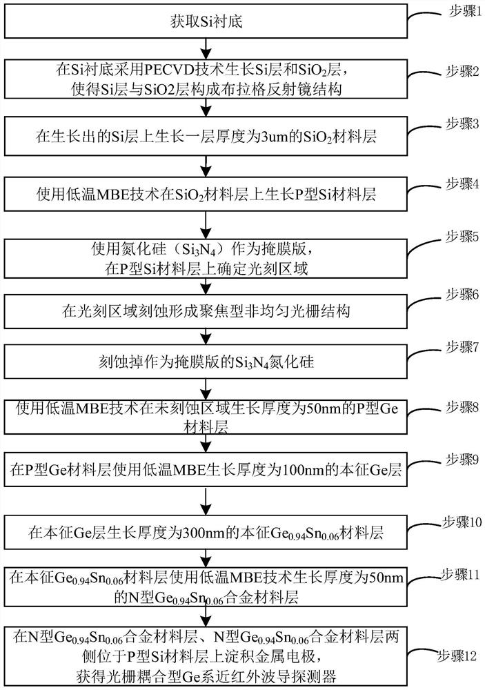
[0051] The present invention will be described in further detail below in conjunction with specific embodiments, but the embodiments of the present invention are not limited thereto.

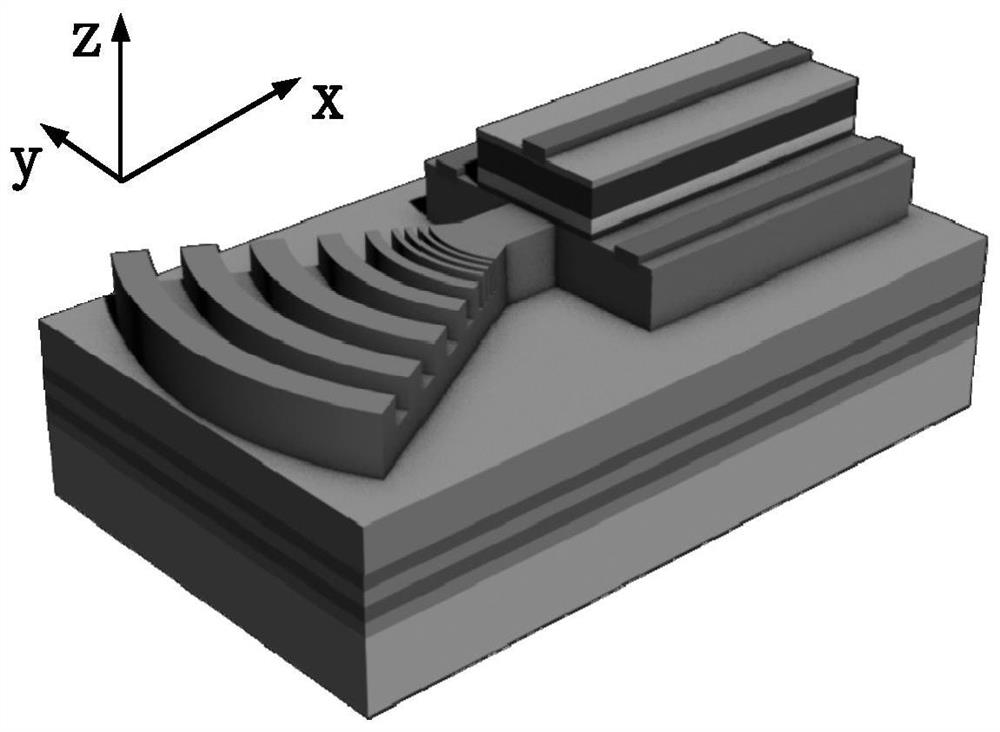
[0052] like figure 1 As shown, a grating-coupled Ge-based near-infrared waveguide detector of the present invention includes:

[0053] The Si substrate, the Si layer and the SiO forming the Bragg mirror structure arranged in order from top to bottom 2 layer, SiO 2 Material layer and P-type Si material layer;

[0054] Focused non-uniform grating structure etched in the etched region on the P-type Si material layer;

[0055] Among them, the focusing non-uniform grating structure is in the shape of a fan ring. In the focusing non-uniform grating structure, the grating is gradually sparse from the inner ring of the fan ring to the outer ring, and the connection between the inner ring of the fan ring and the unetched area presents a cylindrical shape;

[0056] The P-type Ge material layer, the in...


PUM

PropertyMeasurementUnit
thicknessaaaaaaaaaa
thicknessaaaaaaaaaa
thicknessaaaaaaaaaa

Abstract

The invention provides a grating coupling type Ge series near-infrared waveguide detector and a preparation method thereof. A Si layer and a SiO2 layer are enabled to form a Bragg reflector structure by growing the Si layer and the SiO2 layer to improve the coupling efficiency, and a focusing type non-uniform grating structure is formed by etching a P-type Si material layer. A thin Ge material buffer layer with the doping concentration lower than that of a P-type Si material layer is grown between the P-type Si material layer and a GeSn alloy material, the influence of lattice mismatch is reduced, optical loss generated by auger recombination is reduced, the length of a light absorption layer can be reduced through the generated intrinsic Ge0.94Sn0.06 material layer, and the optical detection range can be expanded to be longer. Therefore, the grating coupling type Ge near-infrared waveguide detector not only can solve the problems of low coupling efficiency, low light response and the like of a traditional detector, but also can meet near-infrared spectrum detection, has the characteristics of high speed, high response and easiness in integration with a silicon substrate, and has relatively high photoelectric conversion efficiency and light stability.

Description

technical field [0001] The invention belongs to the technical field of semiconductor optoelectronics, and in particular relates to a grating-coupled Ge-based near-infrared waveguide detector and a preparation method thereof. Background technique [0002] Photodetector is one of Si-based photoelectric active devices, and it is a key module in many application fields. According to the absorption characteristics of different materials for different wavelength bands, the device can realize the detection of light from ultraviolet, visible to infrared. Among them, the near-infrared photodetector in the 1100-2500nm band has a stronger ability to penetrate dense fog and a large amount of dust in the atmosphere than visible light, and can achieve low-loss resolution compared to mid-infrared and far-infrared objects without background objects It has applications in biological sensing and pattern recognition, night vision imaging, atmospheric remote sensing, optical fiber communication...

Claims


Application Information

Patent Timeline
Patent Type & Authority Applications(China)
IPC IPC(8): H01L31/028H01L31/109H01L31/18
CPCH01L31/028H01L31/109H01L31/1812Y02E10/547Y02P70/50
Inventor 舒斌张二同朱佳迪胡辉勇王利明景文龙
Owner XIDIAN UNIV
Why Eureka
Try Eureka