Topological insulator/molybdenum ditelluride heterojunction-based phototransistor, and production method and application thereof
A technology of topological insulator and phototransistor, applied in circuits, electrical components, semiconductor devices, etc., to achieve the effects of high electron mobility, gate voltage controllability, low bias voltage control, and high sensitivity
- Summary
- Abstract
- Description
- Claims
- Application Information
AI Technical Summary
Problems solved by technology
Method used
Image

Examples
Embodiment 1
[0041] 1. SiO 2 / Si substrate is ultrasonicated with acetone, isopropanol, and deionized water for 10 minutes each, and dried with a nitrogen gun;
[0042] 2. With SiO 2 / Si as the substrate and the semiconductor 2H-MoTe prepared by the tape stripping method 2 Nanosheets, 2H-MoTe with a thickness of 10-70nm selected by optical microscope 2 Nanosheets;
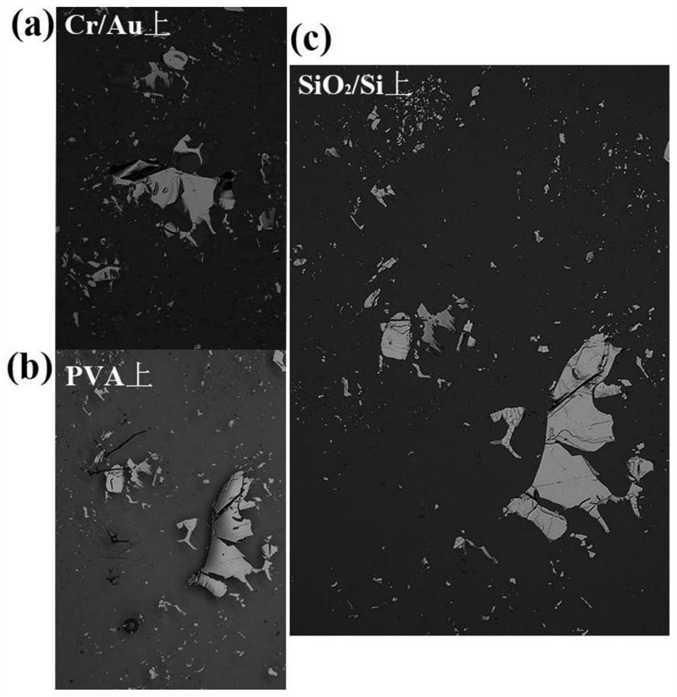
[0043] 3. Evaporate 2nm Ti / 2nmAu onto SiO by electron beam evaporation 2 / Si substrate, the Bi 2 Se 3 The blue tape adheres rapidly to the above Ti / Au SiO 2 / Press on the Si substrate for 1-2 minutes, and slowly peel off to obtain bright-colored Bi 2 Se 3 ; Then by polyvinyl alcohol (PVA) / polymethyl methacrylate (PMMA) transfer method and gold etching solution (KI:I 2 :H 2 The mass ratio of O=4:1:40) to Bi 2 Se 3 Perform transfer and cleaning treatment to obtain a topological insulator Bi with a thickness of 5-300nm 2 Se 3 Nanosheets, Bi with a thickness of about 12nm selected by optical microscopy 2 Se 3 Nanos...
Embodiment 2
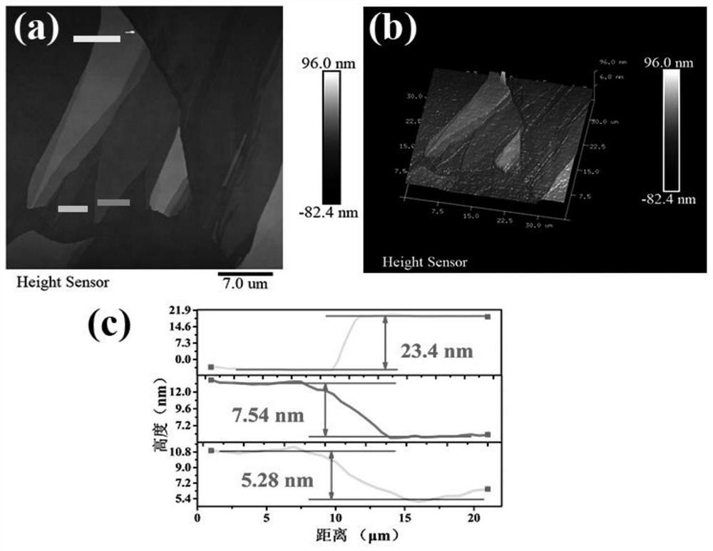
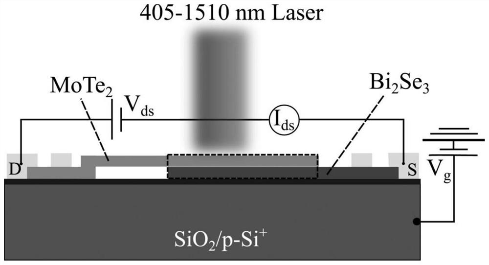
[0052] The difference from Example 1 is: the selected Bi 2 Se 3 The thickness is about 24.8nm, MoTe 2 The thickness is 26.9nm. Figure 9 For the Bi prepared in Example 2 2 Te 3 / 2H-MoTe 2 Optical microscope pictures and electrical performance tests of heterojunction phototransistors. Where (a) is the measured overlapping area of the heterojunction is 234μm 2 , 2H-MoTe 2 Above, Bi 2 Se 3 Below; (b) is Bi 2 Te 3 / 2H-MoTe 2 The current-voltage curve of a heterojunction phototransistor, known as MoTe 2 Anode (Drain), Bi 2 Se 3 Connected to the cathode (Source), it shows that the heterojunction phototransistor exhibits significant reverse rectification behavior, and the rectification ratio (-3 / 3V) is 30. Figure 10 For Bi in Example 2 2 Te 3 / 2H-MoTe 2 The atomic force microscope image of the heterojunction phototransistor, it can be known that Bi 2 Se 3 The thickness is about 24.8nm, 2H-MoTe 2 The thickness is about 26.9nm, indicating that the prepared Bi 2...
Embodiment 3
[0054] The difference from Example 1 is: the selected Bi 2 Se 3 The thickness is about 5.87nm, 2H-MoTe 2 The thickness is about 15.7nm. Figure 11 For the Bi prepared in Example 3 2 Te 3 / 2H-MoTe 2 Optical microscope pictures and electrical performance tests of heterojunction phototransistors. Where (a) is the measured overlapping area of the heterojunction is 20 μm 2 , 2H-MoTe 2 Above, Bi 2 Se 3 Below; (b) the picture shows Bi 2 Te 3 / 2H-MoTe 2 The current-voltage curve of a heterojunction phototransistor, known as MoTe 2 Connect to cathode (Source), Bi 2 Se 3 Connected to the anode (Drain), it shows that the heterojunction phototransistor exhibits significant reverse rectification behavior, and the rectification ratio (-3 / 3V) is 57. Figure 12 For Bi in Example 3 2 Te 3 / 2H-MoTe 2 The atomic force microscope image of the heterojunction phototransistor, it can be known that Bi 2 Se 3 The thickness is about 10.2nm, 2H-MoTe 2 The thickness is about 21.5nm...
PUM
| Property | Measurement | Unit |
|---|---|---|
| Thickness | aaaaa | aaaaa |
| Thickness | aaaaa | aaaaa |
| Thickness | aaaaa | aaaaa |
Abstract
Description
Claims
Application Information
 - R&D
- Intellectual Property
- Life Sciences
- Materials
- Tech Scout
- Unparalleled Data Quality
- Higher Quality Content
- 60% Fewer Hallucinations
Browse by: Latest US Patents, China's latest patents, Technical Efficacy Thesaurus, Application Domain, Technology Topic, Popular Technical Reports.
© 2025 PatSnap. All rights reserved.Legal|Privacy policy|Modern Slavery Act Transparency Statement|Sitemap|About US| Contact US: help@patsnap.com