Molybdenum disulfide/graphene composite heterojunction and preparation method thereof

A graphene composite, molybdenum disulfide technology, applied in ion implantation plating, metal material coating process, coating and other directions, can solve problems such as poor adhesion, reduce poor stability, improve crystal quality, and reduce costs wasteful effect

Active Publication Date: 2022-02-01
XI AN JIAOTONG UNIV +1
View PDF5 Cites 0 Cited by
  • Summary
  • Abstract
  • Description
  • Claims
  • Application Information

AI Technical Summary

Problems solved by technology

Existing carbon-coated base films have poor adhesion to the base

Method used


Image

  • Molybdenum disulfide/graphene composite heterojunction and preparation method thereof
  • Molybdenum disulfide/graphene composite heterojunction and preparation method thereof
  • Molybdenum disulfide/graphene composite heterojunction and preparation method thereof

Examples


Embodiment 1

[0034] The object of the present invention is to provide a kind of magnetron sputtering preparation MoS 2 / Graphene composite heterojunction method to suppress micro-discharge effect.

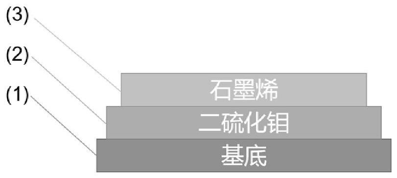
[0035] Step 1: The substrate is ultrasonically cleaned with acetone and alcohol for 20 minutes respectively to remove the adsorption on the surface of the substrate, and blown dry with nitrogen. On the surface of the substrate 1, a molybdenum disulfide buffer layer is deposited on the substrate 1 by means of radio frequency magnetron sputtering molybdenum disulfide target. The working pressure in the cavity is 4Pa, and the thickness of the deposited molybdenum disulfide buffer layer is 10nm;

[0036] Step 2: close the argon gas valve, stop feeding the argon gas with a flow rate of 25 sccm, and feed methane into the coating chamber with a flow rate of 30 sccm, so that the working pressure in the coating chamber is 7Pa, and the thickness of the deposited graphene is 15nm;

[0037] Step 3: Perform...

Embodiment 2

[0039] The object of the present invention is to provide a kind of magnetron sputtering preparation MoS 2 / Graphene composite heterojunction method to suppress micro-discharge effect.

[0040] Step 1: The substrate is ultrasonically cleaned with acetone and alcohol for 20 minutes respectively to remove the adsorption on the surface of the substrate, and blown dry with nitrogen. On the surface of the substrate 1, a molybdenum disulfide buffer layer is deposited on the substrate 1 by radio frequency magnetron sputtering molybdenum disulfide target. The working pressure in the cavity is 10Pa, and the thickness of the deposited molybdenum disulfide buffer layer is 10nm;

[0041] Step 2: close the argon gas valve, stop feeding the argon gas with a flow rate of 30 sccm, and feed methane into the coating chamber with a flow rate of 50 sccm, so that the working pressure in the coating chamber is 10 Pa, and the thickness of the deposited graphene is 15 nm;

[0042] Step 3: Perform hi...

Embodiment 3

[0044] The object of the present invention is to provide a kind of magnetron sputtering preparation MoS 2 / Graphene composite heterojunction method to suppress micro-discharge effect.

[0045] Step 1: The substrate is ultrasonically cleaned with acetone and alcohol for 20 minutes respectively to remove the adsorption on the surface of the substrate, and blown dry with nitrogen. On the surface of the substrate 1, a molybdenum disulfide buffer layer is deposited on the substrate 1 by using radio frequency magnetron sputtering molybdenum disulfide target mode. The working pressure in the cavity is 1Pa, and the thickness of the deposited molybdenum disulfide buffer layer is 10nm;

[0046] Step 2: close the argon gas valve, stop feeding the argon gas with a flow rate of 10 sccm, and feed methane into the coating chamber with a flow rate of 20 sccm, so that the working pressure in the coating chamber is 1Pa, and the thickness of the deposited graphene is 15nm;

[0047] Step 3: Per...


PUM

PropertyMeasurementUnit
thicknessaaaaaaaaaa
thicknessaaaaaaaaaa

Abstract

The invention discloses a molybdenum disulfide/graphene composite heterojunction and a preparation method thereof. The molybdenum disulfide/graphene composite heterojunction comprises a substrate 1, a molybdenum disulfide layer 2 and a graphene layer 3, wherein the molybdenum disulfide layer 2 is arranged on the substrate 1, and the graphene layer is arranged on the molybdenum disulfide layer 2. According to the preparation method, the sulfur vacancy of the prefabricated thin film is reduced and the crystallization quality of the molybdenum disulfide buffer layer is improved by optimizing the design of the process of preparing the MoS2/graphene composite heterojunction through magnetron sputtering and combining the annealing process, and meanwhile, the composite heterojunction thin film with high surface roughness is formed on the carbon film through argon ion sputtering; the average collision frequency of the secondary electrons and the surface trap wall can be effectively increased, so that the secondary electron emission phenomenon is inhibited.

Description

technical field [0001] The invention belongs to the technical field of carbon-based materials, in particular to a molybdenum disulfide / graphene composite heterojunction and a preparation method thereof. Background technique [0002] Secondary electron emission is also known as the electron multiplication effect. The emission process of secondary electrons mainly includes three parts: ① the initial electrons enter the interior of the material and excite the internal secondary electrons, ② the excited internal secondary electrons move to the surface, and ③ move to the surface. The internal secondary electrons on the surface overcome the surface barrier and emerge as true secondary electrons. [0003] In recent years, although my country has made significant progress in the design of communication, aerospace and satellite high-power components, the electron multiplication effect is still a bottleneck restricting the power capacity of microwave components, and it is also an impo...

Claims


Application Information

Patent Timeline
Patent Type & Authority Applications(China)
IPC IPC(8): C23C14/06C23C14/35C23C14/58C23C14/02
CPCC23C14/35C23C14/0623C23C14/5806C23C14/5826C23C14/0605C23C14/024
Inventor 胡忠强赵亚楠吴金根彭淑婷刘明何鋆杨晶张毅崔万照
Owner XI AN JIAOTONG UNIV
Why Eureka
Try Eureka