
Copper alloy thin film, protective layer and preparation method based on copper alloy thin film after service

A copper alloy and protective layer technology, applied in the field of electronic thin film materials, can solve the problems of failure of electronic equipment, electrochemical migration of copper, incomplete coverage of silver plating, etc., so as to improve the service life, simplify the process, and inhibit electrochemical migration. Effect

Active Publication Date: 2022-05-17
JIANGSU UNIV OF SCI & TECH
View PDF1 Cites 0 Cited by
  • Summary
  • Abstract
  • Description
  • Claims
  • Application Information

AI Technical Summary

Problems solved by technology

However, the process characteristics of immersion silver technology make the silver plating layer on the immersion silver printed circuit board very thin, with many tiny holes, and the silver plating layer cannot completely cover the substrate metal.
Therefore, although the printed circuit board is treated with immersion silver, the silver coating will electrochemically react with the substrate metal copper under certain humidity and temperature conditions, causing electrochemical migration of copper, resulting in electronic equipment failure.

Method used


Image

  • Copper alloy thin film, protective layer and preparation method based on copper alloy thin film after service
  • Copper alloy thin film, protective layer and preparation method based on copper alloy thin film after service
  • Copper alloy thin film, protective layer and preparation method based on copper alloy thin film after service

Examples


Embodiment 1

[0035] Copper-molybdenum alloy is electrodeposited on the printed circuit board, and then the alloy coating is layered to form defects such as corrosion and migration damage to protect the metal copper during service, so as to improve circuit reliability. The specific steps include:

[0036] 1) Prepare electroplating solution: 87g / L citric acid (C 6 h 8 o 7 ), 40g / L copper sulfate (CuSO 4 ), 160g / L sodium molybdate (Na 2 MoO 4 ·H 2 O) and 0.2g / L sodium lauryl sulfate (C 12 h 25 SO 4 Na) was added into deionized water and stirred evenly to obtain the electroplating solution;

[0037] 2) Pretreatment of electroplating: use 1500, 2000 mesh metallographic sandpaper to polish the surface of the copper plate smooth, and clean it with deionized water and absolute ethanol, and then dry to obtain the substrate to be plated;

[0038] 3) Electrodeposition: use the substrate to be plated prepared in step 2) as the cathode, and the carbon plate as the anode, put the anode and the ...

Embodiment 2

[0045] The copper-chromium alloy formed by the method of magnetron sputtering on the circuit board, the specific steps include:

[0046] During the magnetron sputtering process, the purity of the Cu target material is 99.99%, the purity of the Cr target material is 99.9%; the basic vacuum degree is 10 -7 Torr, maintain argon protection during the sputtering process, and keep the argon pressure at 10 -3 Torr; a Cu-4.2Cr film with a mass percent content of 4.2% was obtained.

[0047] see Figure 7 The XRD results show that the peak is basically copper, but the width of the peak increases, which should be that Cr is physically mixed with Cu during the sputtering process.

[0048] Since the structure is thermodynamically unstable, further applying a temperature field to the film, that is, after thermal aging treatment at a temperature of 60°C for 12 hours, Cr will precipitate on the surface of Cu at this time, forming a thin continuous Cr layer, which is to protect the Cu layer...

Embodiment 3

[0050] Since the cold rapid solidification largely expands the solid solubility of Co in the Cu phase from 7.46% to 20% under equilibrium conditions, Cu-Co of different compositions has positive mixing enthalpy, and there is a metastable phase in the phase diagram Solubility gap, which makes the solid solubility of Cu-Co alloy have a huge space under supersaturated conditions.

[0051] Electrodepositing a copper-cobalt alloy coating on a copper plate comprises the following steps:

[0052] 1) Preparation of electroplating solution: take 0.01mol of copper sulfate, 0.7mol of cobalt sulfate and 0.2mol of sodium acetate and add them into deionized water and stir evenly to prepare the electroplating solution;

[0053] 2) Pretreatment of electroplating: use 1500, 2000 mesh metallographic sandpaper to polish the surface of the copper plate smooth, and clean it with deionized water and absolute ethanol, and then dry to obtain the substrate to be plated;

[0054] 3) Electrodeposition:...


PUM


Abstract

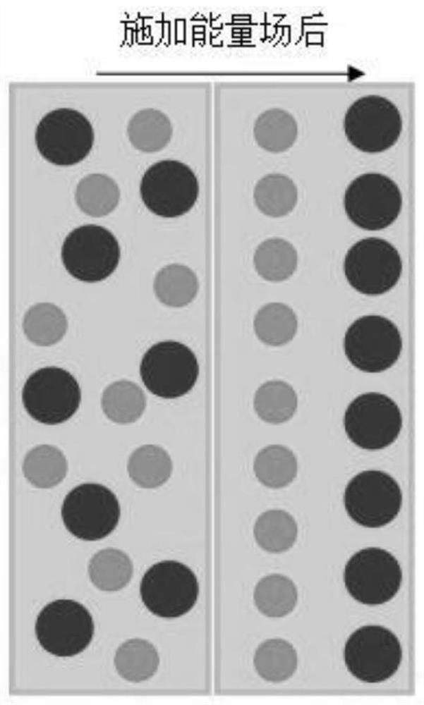
The invention discloses a copper alloy thin film, a protective layer based on the copper alloy thin film after service and a preparation method. The copper alloy thin film is a binary alloy, including copper elements and additive elements that can form positive mixing entropy with copper; The mass percentage is 95~99wt%; by first forming a copper alloy film with positive mixing enthalpy on the substrate; and then applying an energy field to the copper alloy film to precipitate the added elements and form a protective layer on the surface of the copper film. The present invention adopts the copper alloy thin film with positive mixing enthalpy, causes the added elements in the alloy to move to the surface through the action of the pressure difference, and finally makes the added elements cover the copper, inhibits the electrochemical migration of metal copper, and improves the copper circuit board. Resistance to electrochemical migration, the overall preparation method can form a dual-element coating at one time, which simplifies the process and improves the reliability of the coating.

Description

technical field [0001] The invention belongs to electronic thin film materials, and in particular relates to a copper alloy thin film, a protective layer and a method formed on the surface of a copper circuit board and a copper substrate welding pad based on the copper alloy thin film. Background technique [0002] With the development of science and technology, people's demand for portable electronic products is increasing day by day, and thin, light and small electronic products can be more available in the market, which makes printed circuit boards become smaller and more densely integrated. At the same time, the working conditions of electronic components are getting worse when they are in service, and they often work for a long time under high temperature, high humidity and high voltage. In recent years, corrosion failures have been found between leads on printed circuit boards. Due to the small spacing between the leads on the high-density integrated printed circuit b...

Claims


Application Information

Patent Timeline
Patent Type & Authority Patents(China)
IPC IPC(8): C22C9/00C22C9/06C25D3/58C25D7/00C23C14/35C23C14/16H05K1/02H05K3/22
CPCC22C9/00C22C9/06C25D3/58C25D7/00C23C14/35C23C14/165H05K1/02H05K3/22H05K3/282H05K1/09C25D5/48C25D5/56C23C14/205C23C14/5806
Inventor 王小京丁梓峰李溯杰高幸刘瑞刘宁
Owner JIANGSU UNIV OF SCI & TECH
Learn More