Preparation method of PDMS in-situ wrinkled antireflection film and preparation method of white organic light-emitting diode

A technology of light-emitting diodes and anti-reflection coatings, which is applied in semiconductor/solid-state device manufacturing, electrical components, and electrical solid-state devices. It can solve problems such as unsuitable flexible substrates, harsh reaction conditions, and expensive equipment, and achieve improved display quality and cost. Low, soft output light effect

Pending Publication Date: 2022-03-18
SHANGHAI UNIV
View PDF0 Cites 0 Cited by
  • Summary
  • Abstract
  • Description
  • Claims
  • Application Information

AI Technical Summary

Problems solved by technology

The external light extraction mainly includes the introduction of diffraction gratings, light scattering media, anode surface patterns, microlenses, scattering films, sandblasting, multi-layer stepped films, etc. outside the device. Most of the above technologies involve complex processes such as multiple pattern transfers, or Need expensive equipment, harsh reaction conditions, high cost or not suitable for flexible substrates and other disadvantages

Method used


Image

  • Preparation method of PDMS in-situ wrinkled antireflection film and preparation method of white organic light-emitting diode
  • Preparation method of PDMS in-situ wrinkled antireflection film and preparation method of white organic light-emitting diode
  • Preparation method of PDMS in-situ wrinkled antireflection film and preparation method of white organic light-emitting diode

Examples


Embodiment 1

[0064] In this example,

[0065] see figure 1 and figure 2 , a method for preparing a PDMS in-situ wrinkled anti-reflection film and a white light organic light-emitting diode, comprising the steps of:

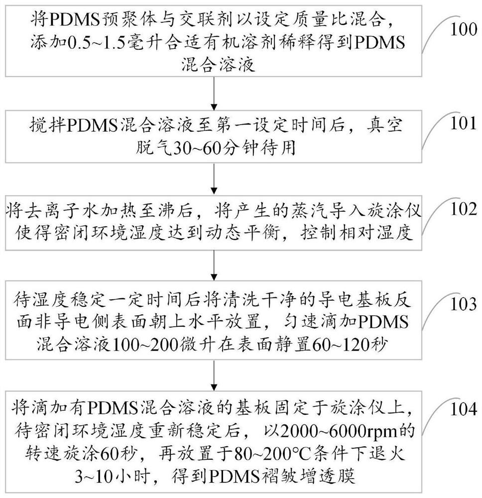
[0066] Step 100: According to the mass ratio (w / w) of DMS prepolymer and crosslinking agent mixed at 10:1, weigh 3.3g of PDMS prepolymer and PDMS crosslinking agent, and add them into a clean transparent reagent bottle , respectively take 0.5mL, 1.0mL and 1.5mL of chloroform and mix with PDMS solution;

[0067] Step 101: Stir evenly, seal, and place the mixed solution in a moderate vacuum environment for degassing for 1 hour;

[0068] Step 102: After heating the deionized water to boiling, the generated steam is introduced into the spin coater so that the humidity in the airtight environment reaches a dynamic balance, and the relative humidity is controlled to be 75%;

[0069] Step 103: After ultrasonically cleaning the ITO glass substrate with detergent, acetone, deioniz...

Embodiment 2

[0077] This embodiment is basically the same as Embodiment 1, and the special features are:

[0078] In this embodiment, a method for preparing a PDMS in-situ wrinkled anti-reflection film and a white light organic light-emitting diode includes the following steps:

[0079] Step 100: According to the mass ratio (w / w) of DMS prepolymer and crosslinking agent mixed at 10:1, weigh 3.3g of PDMS prepolymer and PDMS crosslinking agent, and add them into a clean transparent reagent bottle , take 1.0mL chloroform and mix it with PDMS solution;

[0080] Step 101 to step 200: this step is the same as that of Embodiment 1;

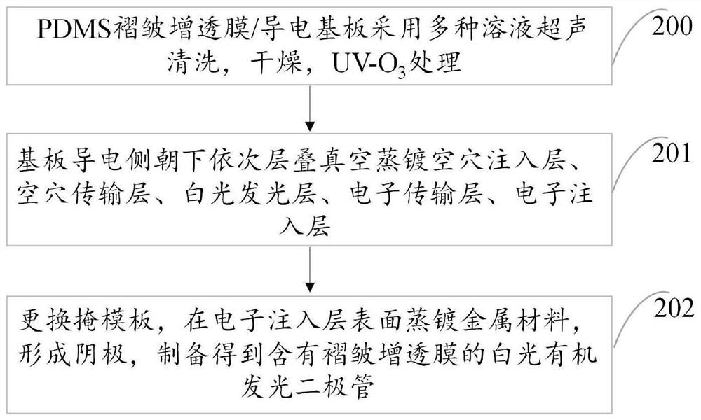
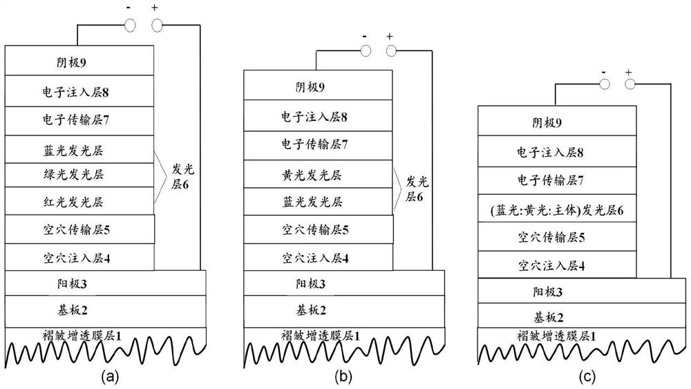
[0081] Step 201: Place the conductive side of the substrate in step 200 down in a vacuum evaporation chamber to sequentially evaporate various functional layers, including NPB:rubrene (2wt%, 50nm) / BCP (8nm) / Alq3 (30nm) / Liq ( 1nm);

[0082] Step 202: Finally, replace the mask to vapor-deposit cathode metal Al to prepare an electrode cathode layer with a thickness o...


PUM

PropertyMeasurementUnit
thicknessaaaaaaaaaa
thicknessaaaaaaaaaa
thicknessaaaaaaaaaa

Abstract

The invention discloses a PDMS in-situ wrinkle antireflection film and a preparation method of a white light organic light-emitting diode, which is based on a physical and chemical process between volatilization of an organic solvent on the surface of a polymer and condensation of water vapor on the surface of the PDMS polymer, and is combined with compression stress generated by spin coating to enable a film epidermis layer to be unstable and cooperatively generate a wrinkle structure. Water molecules serve as a mother set in a traditional method, after water vapor is evaporated and dried, the mother set is automatically removed, a wrinkled unit structure is obtained, in-situ film forming is conducted on the non-conductive side of the conductive substrate through the method, and the film serves as an antireflection film of a white light organic light emitting diode (OLED). According to the method, the optical refraction and total reflection resistance of the wrinkled rough surface are utilized, so that the emergent light of the white light OLED is softer, the visual brightness is enhanced, and the method is a simple and efficient in-situ anti-reflection method. Compared with the prior art, the preparation method of the OLED wrinkle antireflection film provided by the invention has the characteristics of simple process, low cost, adjustable size and the like, so that the emergent light of a white light OLED applying the PDMS wrinkle antireflection film is remarkably enhanced.

Description

technical field [0001] The invention relates to the technical field of nano-processing and light-emitting diode preparation, in particular to a PDMS in-situ wrinkled anti-reflection film and a preparation method of a white light organic light-emitting diode. Background technique [0002] Organic light-emitting diodes (organic light-emitting diodes, OLEDs) have shown great application potential in the fields of full-color flat panel displays and solid-state lighting due to their advantages such as self-illumination, wide viewing angle, rich colors, and low-voltage DC drive. Although the internal quantum efficiency of OLED is almost close to 100%, due to the light loss caused by waveguide mode, substrate mode and plasmon mode, about 80% of the photons emitted by the organic light-emitting layer are confined inside the device, and only about 20% of the photons The external quantum efficiency of the device is greatly lower than the internal quantum efficiency. Therefore, enhanci...

Claims


Application Information

Patent Timeline
Patent Type & Authority Applications(China)
IPC IPC(8): H01L51/56H01L51/52
CPCH10K50/858H10K71/00
Inventor 郑燕琼陈与欢陈俊聪李维光陈维安
Owner SHANGHAI UNIV
Why Eureka
Try Eureka