

Method for simultaneously improving open-circuit voltage and stability of full-suede perovskite/crystalline silicon laminated solar cell
A solar cell and open-circuit voltage technology, applied in the field of solar cells, can solve the problems of limited charge transmission, easy phase transition, excessive guanidine ion radius, etc., and achieve the effect of simple preparation method and low difficulty in operation process
- Summary
- Abstract
- Description
- Claims
- Application Information
AI Technical Summary
Problems solved by technology
Method used
Image

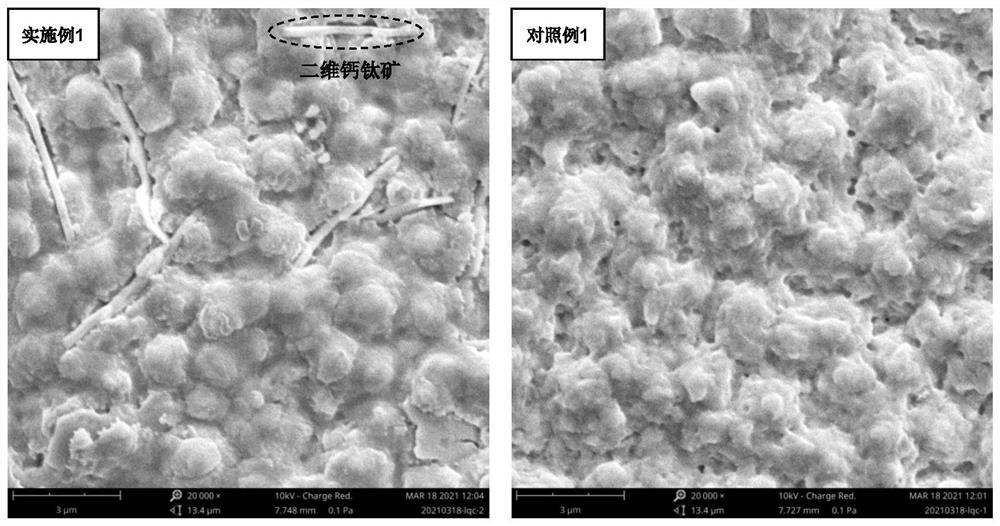
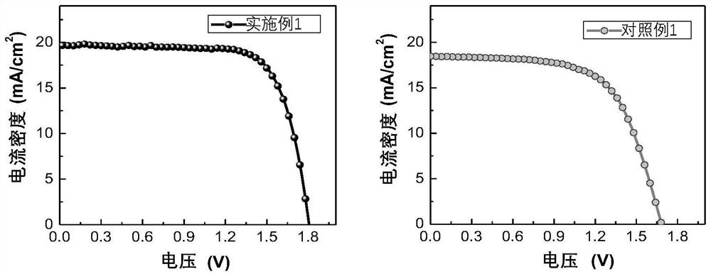
Examples
Embodiment 1
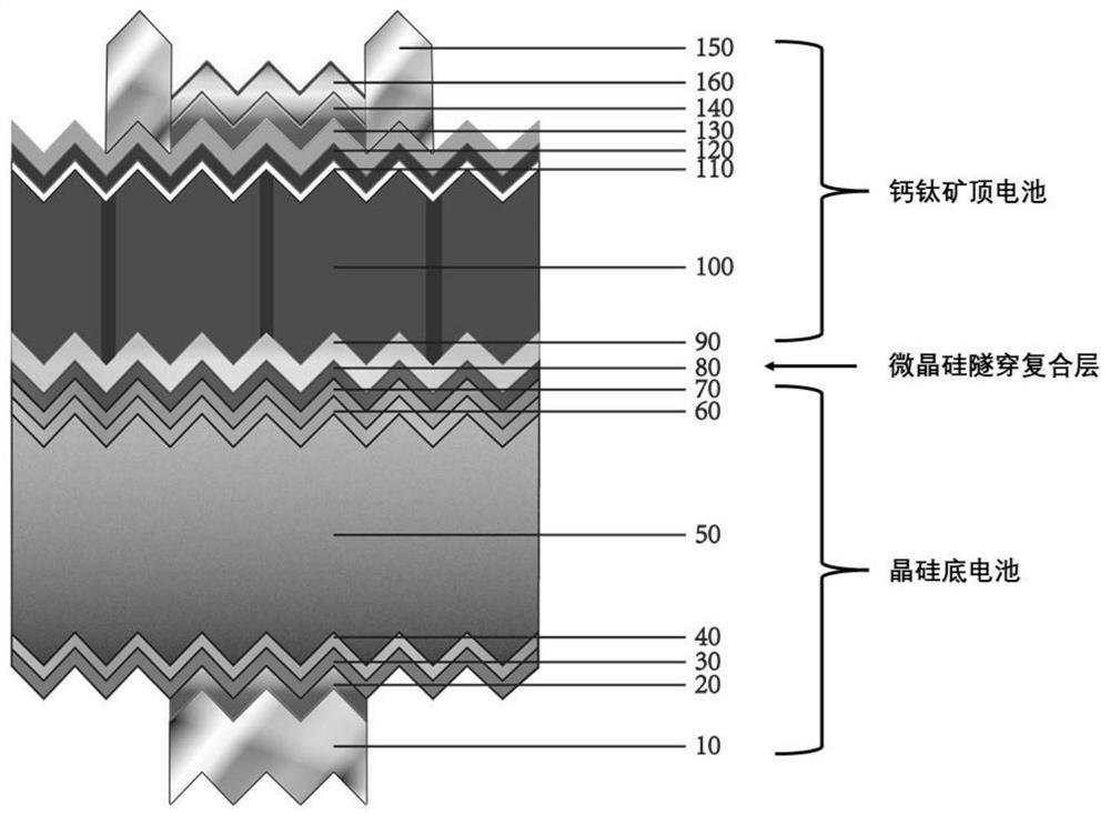
[0034] A kind of embodiment of the method that improves full textured perovskite / crystalline silicon laminated solar cell open circuit voltage and stability simultaneously, comprises the steps:
[0035] (1) Select a commercial micron-scale suede intrinsic monocrystalline silicon wafer (resistance 1-3Ω, 150 microns), and deposit 5nm intrinsic Amorphous silicon and 10nm p-type amorphous silicon, and then sequentially deposit 5nm intrinsic amorphous silicon and 10nm n-type amorphous silicon on the front of the intrinsic single crystal silicon wafer, wherein the intrinsic amorphous silicon reacts to the equipment Intraluminal SiH 4 (flow 20sccm) and H 2 (Flow rate 50sccm), intrinsic amorphous silicon can be obtained under the action of plasma. When p-type amorphous silicon is deposited, additional B 2 h 6 (Flow 20sccm) gas, during the deposition of n-type amorphous silicon, additional PH is required 3 (Flow 20sccm) Gas. Next, a 100 nm rear indium tin oxide transparent electro...
PUM
| Property | Measurement | Unit |
|---|---|---|
| Thickness | aaaaa | aaaaa |
| Thickness | aaaaa | aaaaa |
| Thickness | aaaaa | aaaaa |
Abstract
Description
Claims
Application Information