Application of compound in solar cell
A technology of solar cells and compounds, applied in the field of solar cells, can solve the problems of low performance of cell devices and decreased device efficiency, and achieve the effects of improving interface contact, improving efficiency and stability, and increasing adhesion
- Summary
- Abstract
- Description
- Claims
- Application Information
AI Technical Summary
Problems solved by technology
Method used
Image
Examples
preparation example Construction
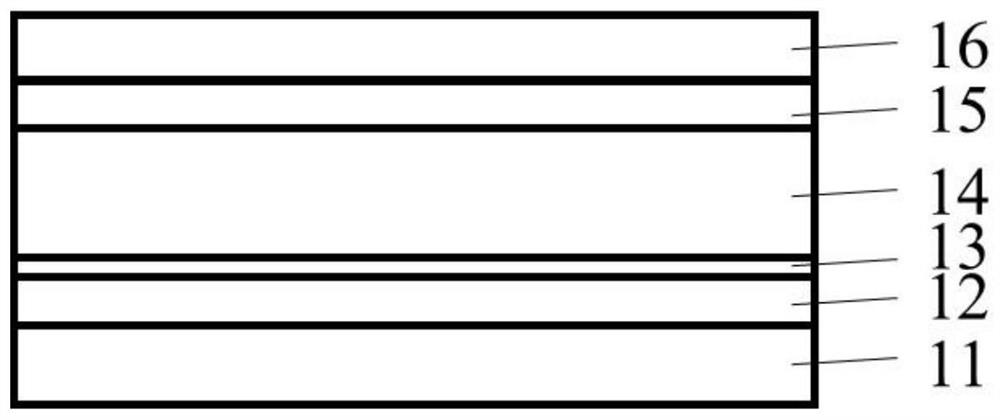
[0069] The application provides a method for preparing a solar cell, comprising the steps of:
[0070] Step 1: providing a bottom electrode 11;
[0071] Step 2: preparing a first carrier transport layer 12 on one side surface of the bottom electrode 11;
[0072] Step 3: preparing a modification layer 13 on the surface of the first carrier transport layer 12 facing away from the bottom electrode 11;
[0073] Step 4: preparing a perovskite absorption layer 14 on the surface of the modification layer 13 facing away from the first carrier transport layer 12;
[0074] Step 5: preparing a second carrier transport layer 15 on the surface of the perovskite absorption layer 14 away from the modification layer 13;
[0075] Step 6: preparing a top electrode 16 on the surface of the second carrier transport layer 15 facing away from the perovskite absorption layer 14;
[0076] The modification layer 13 is a (G1)n-R-(G2)m layer;
[0077] The (G1)n-R-(G2)m layer is formed from the afore...
Embodiment 1
[0112] The preparation method of the solar cell of the present embodiment comprises the following steps:
[0113] Preparation of Bottom Electrode 11
[0114] On the glass substrate, an FTO (fluorine-doped tin oxide) transparent conductive layer is deposited by APCVD (atmospheric pressure chemical vapor deposition) method, thereby forming the bottom electrode 11; the thickness of the transparent conductive layer is 400nm; the square resistance is 10Ω / sq; Then cut into 2cm × 2cm size, wash clean.
[0115] Preparation of the first carrier transport layer 12
[0116] On the surface of the transparent conductive layer away from the glass substrate, a nickel oxide layer, that is, the first carrier transport layer 12, is prepared by PVD sputtering. The specific process parameters are 99.99% Ni target material, and the deposition pressure is -4 Pa, power 50-1000W, O 2 The partial pressure is about 3%-20%. The first carrier transport layer 12 is a hole transport layer with a thicknes...
Embodiment 2
[0127] The difference between Example 2 and Example 1 lies in the modification layer 13. The modification layer 13 in Example 2 is modified by anthracene-2,6-dicarboxylic acid (abbreviated as ADCA, purity: 95%, purchased from McLean) Layer 13 with a thickness of 5 nm.
[0128] The performance of the solar cell is shown in Table 1.
PUM
| Property | Measurement | Unit |
|---|---|---|
| thickness | aaaaa | aaaaa |
| thickness | aaaaa | aaaaa |
| thickness | aaaaa | aaaaa |
Abstract
Description
Claims
Application Information


