Lead-free perovskite material and preparation method and application thereof
A technology of perovskite and titanium, which is applied in chemical instruments and methods, semiconductor/solid-state device manufacturing, antimony compounds, etc., can solve the problems of low device efficiency and solar cell device efficiency, and achieve good switching response repeatability, Solve toxicity and stability problems, good stability effect
- Summary
- Abstract
- Description
- Claims
- Application Information
AI Technical Summary
Problems solved by technology
Method used
Image
Examples
Embodiment 1
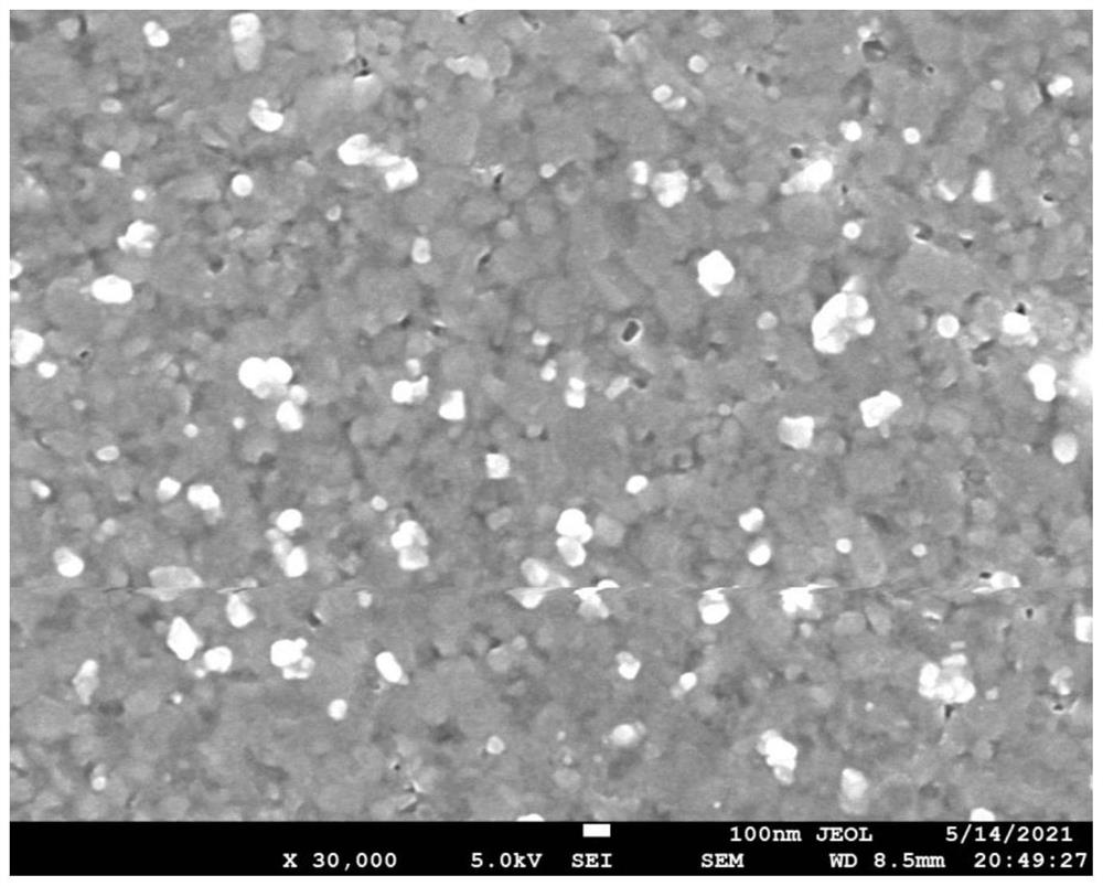
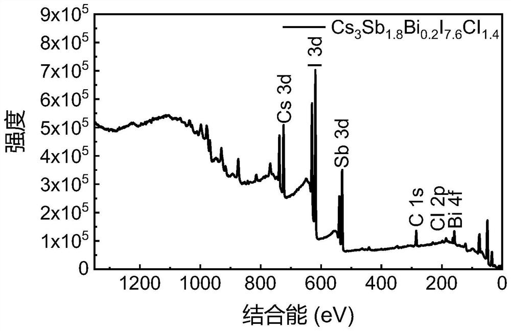
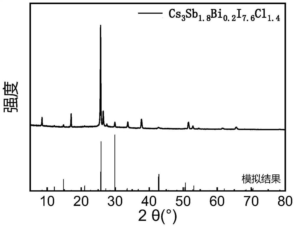
[0037] Lead-free perovskite material Cs 3 Sb 1.8 Bi 0.2 I 7.6 Cl 1.4 Preparation of the film:
[0038]Cut ITO transparent conductive glass with a size of 20 × 20mm with a glass knife, and then ultrasonically clean the cut ITO transparent conductive glass substrate with glass cleaner, deionized water, isopropanol, and ethanol, and then blow it with nitrogen. Dry, followed by UV ozone treatment to improve the wettability and cleanliness of the ITO glass surface. Configure 0.6mol / L non-lead perovskite precursor solution, the concentration is calculated as the sum of bismuth and antimony content, specifically including solute cesium iodide, antimony iodide, bismuth iodide, antimony chloride, the concentration is 0.90mol / L respectively , 0.40mol / L, 0.06mol / L, 0.14mol / L, the solvent is dimethyl sulfoxide (DMSO), and it is stirred at room temperature to dissolve it completely. The precursor solution was deposited on the ITO substrate using a spin coater (KW-4A type desktop spin...
Embodiment 2
[0040] Based on lead-free perovskite material Cs 3 Sb 1.8 Bi 0.2 I 7.6 Cl 1.4 Thin-film photovoltaic devices:
[0041] Cut the FTO transparent conductive glass with a size of 20×20mm with a glass knife, and then ultrasonically clean the cut FTO transparent conductive glass substrate with glass cleaning agent, deionized water, isopropyl alcohol, and ethanol, and dry it with nitrogen. , followed by UV ozone treatment to improve the wettability and cleanliness of the FTO glass surface. An electron transport layer titanium dioxide is then deposited on the surface of the FTO. The configuration of the perovskite precursor is the same as in Example 1. 50μl of the prepared precursor solution was spin-coated on the ITO or FTO glass deposited with the electron transport layer using a spin coater. In the auxiliary equipment (DL-10A quartz vacuum gauge and vacuum pump), low-pressure (vacuum degree of 10Pa) treatment is carried out for 60 seconds to make the solvent volatilize quick...
Embodiment 3
[0043] Based on lead-free perovskite material Cs 3 Sb 1.8 Bi 0.2 I 7.6 Cl 1.4 The thin film photodetector:
[0044] Cut ITO transparent conductive glass with a size of 20 × 20 mm with a glass knife, and then ultrasonically clean the cut ITO transparent conductive glass substrate with glass cleaning agent, deionized water, isopropyl alcohol, and ethanol, and blow it with nitrogen. Dry, followed by UV ozone treatment to improve the wettability and cleanliness of the ITO glass surface. Then the hole transport layer nickel oxide nanoparticles were deposited on the surface of ITO. The configuration of the perovskite precursor is the same as in Example 1. 50 μl of the prepared precursor solution was spin-coated on the ITO glass deposited with the hole transport layer using a spin coater. The spin speed of the spin coater was 4000 rmp and the spin time was 30 seconds. In the equipment (DL-10A quartz vacuum gauge and vacuum pump), a low-pressure (vacuum degree of 10Pa) treatmen...
PUM
| Property | Measurement | Unit |
|---|---|---|
| thickness | aaaaa | aaaaa |
| thickness | aaaaa | aaaaa |
Abstract
Description
Claims
Application Information
 - R&D Engineer
- R&D Manager
- IP Professional
- Industry Leading Data Capabilities
- Powerful AI technology
- Patent DNA Extraction
Browse by: Latest US Patents, China's latest patents, Technical Efficacy Thesaurus, Application Domain, Technology Topic, Popular Technical Reports.
© 2024 PatSnap. All rights reserved.Legal|Privacy policy|Modern Slavery Act Transparency Statement|Sitemap|About US| Contact US: help@patsnap.com


