Ultraviolet light-emitting diode epitaxial wafer preparation method for improving hole quantity and epitaxial wafer

A technology of light-emitting diodes and epitaxial wafers, applied in chemical instruments and methods, semiconductor/solid-state device manufacturing, crystal growth, etc. Low luminous efficiency and other issues, to achieve the effect of reducing the probability of capture, uniform distribution, and reduced viscosity

Pending Publication Date: 2022-07-29
HC SEMITEK SUZHOU
View PDF0 Cites 0 Cited by
  • Summary
  • Abstract
  • Description
  • Claims
  • Application Information

AI Technical Summary

Problems solved by technology

[0003] Due to the large forbidden band width of AlGaN material itself, the donor / acceptor energy levels between the band gaps are deepened, and the ionization energy of dopants also increases accordingly, resulting in very low activation rate and carrier concentration of dopant elements.
Moreover, the activation energy of the Mg acceptor doped in the P-type AlGaN layer is high, which can reach 500-600meV, which leads to a very low activation rate of Mg in the P-type AlGaN layer, which will directly affect the P-type AlGaN layer. The amount of holes in the AlGaN layer leads to a lower luminous efficiency of the obtained UV light-emitting diodes

Method used


Image

  • Ultraviolet light-emitting diode epitaxial wafer preparation method for improving hole quantity and epitaxial wafer
  • Ultraviolet light-emitting diode epitaxial wafer preparation method for improving hole quantity and epitaxial wafer
  • Ultraviolet light-emitting diode epitaxial wafer preparation method for improving hole quantity and epitaxial wafer

Examples


Embodiment Construction

[0029] In order to make the objectives, technical solutions and advantages of the present disclosure clearer, the embodiments of the present disclosure will be further described in detail below with reference to the accompanying drawings.

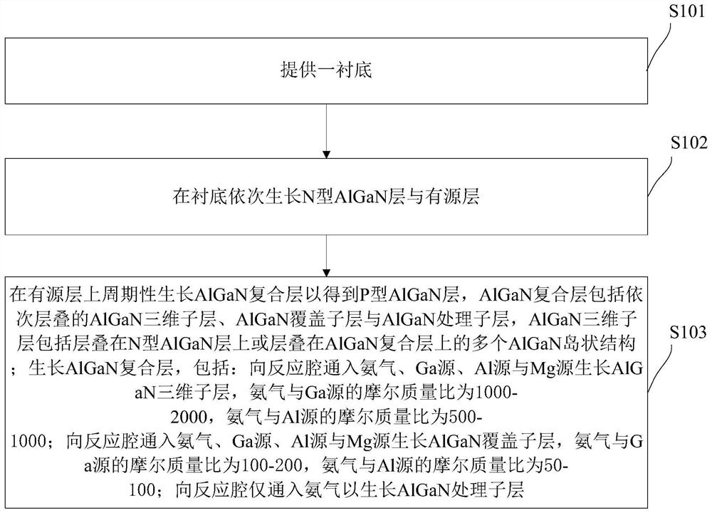
[0030] figure 1 This is a flow chart of a method for preparing an ultraviolet light emitting diode epitaxial wafer with increased hole content provided by an embodiment of the present disclosure. Refer to figure 1 It can be seen that the embodiments of the present disclosure provide a method for preparing an ultraviolet light emitting diode epitaxial wafer with increased hole content, and the method for preparing an ultraviolet light emitting diode epitaxial wafer with increased hole content includes:

[0031] S101: Provide a substrate.

[0032] S102 : growing an N-type AlGaN layer and an active layer sequentially on the substrate.

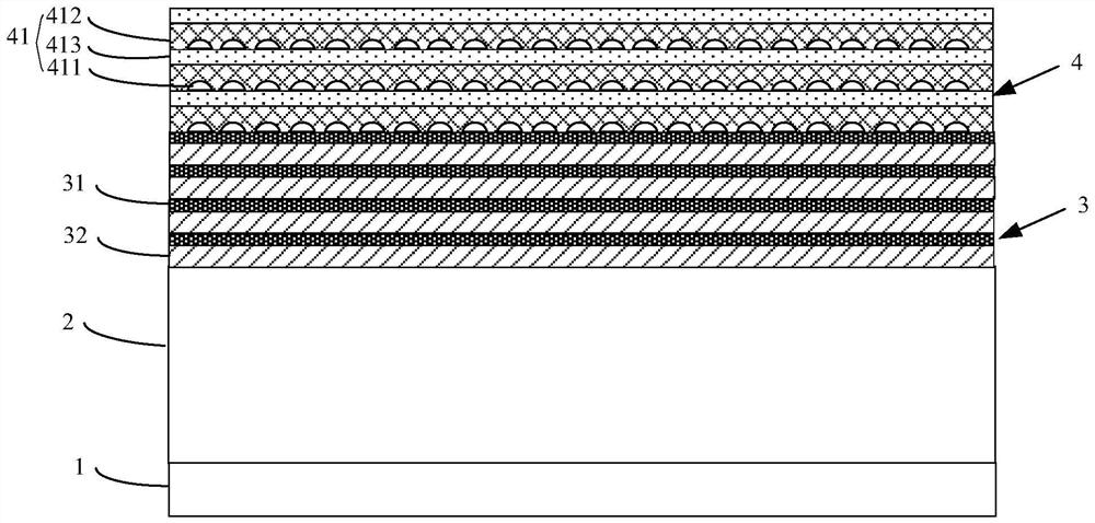
[0033] S103: Periodically growing an AlGaN composite layer on the active layer to obtain a P-type AlGaN la...


PUM

PropertyMeasurementUnit
thicknessaaaaaaaaaa
thicknessaaaaaaaaaa
thicknessaaaaaaaaaa

Abstract

The invention provides a preparation method of an ultraviolet light-emitting diode epitaxial wafer for improving the hole quantity and the epitaxial wafer, and belongs to the technical field of semiconductor devices. And periodically growing an AlGaN composite layer on the active layer to obtain a P-type AlGaN layer, wherein the AlGaN composite layer comprises an AlGaN three-dimensional sub-layer, an AlGaN covering sub-layer and an AlGaN processing sub-layer which are stacked in sequence. And internal stress and defects are reduced. More Mg elements can be more easily doped into the AlGaN three-dimensional sub-layer rich in nitrogen elements, and the hole quantity is increased. The distribution of Al atoms and Ga atoms in a low-nitrogen environment is more uniform, and the crystal quality of the finally obtained AlGaN composite layer is ensured. And finally, only ammonia gas is introduced into the reaction cavity to grow an AlGaN processing sub-layer. It is guaranteed that the finally obtained P-type AlGaN layer can provide a large number of holes, and meanwhile the crystal quality of the finally obtained P-type AlGaN layer is guaranteed.

Description

technical field [0001] The present disclosure relates to the technical field of semiconductor devices, and in particular, to a method for preparing an epitaxial wafer of an ultraviolet light emitting diode and an epitaxial wafer for increasing the amount of holes. Background technique [0002] With the development of light-emitting diode applications, the market demand for ultraviolet light-emitting diodes is increasing, and ultraviolet light-emitting diodes with light-emitting wavelengths covering 210-400nm have advantages that traditional ultraviolet light sources cannot match. Ultraviolet light-emitting diodes are often used in lighting, biomedicine, anti-counterfeiting identification, air, water purification, biochemical testing, high-density information storage, etc. The ultraviolet light emitting diode epitaxial wafer is the basis for preparing the ultraviolet light emitting diode. The ultraviolet light emitting diode epitaxial wafer includes a substrate and an N-type ...

Claims


Application Information

Patent Timeline
Patent Type & Authority Applications(China)
IPC IPC(8): H01L33/00H01L33/12H01L33/14H01L21/02C30B25/16C30B29/40
CPCH01L33/0075H01L33/12H01L33/14H01L21/0254H01L21/0262H01L21/02458C30B25/16C30B29/403
Inventor 蒋媛媛胡烨伟许杨李翠玲从颖李鹏
Owner HC SEMITEK SUZHOU
Why Eureka
Try Eureka