

Novel electro-laser device based on nanorod
A technology of laser devices and nanorods, which is applied in the laser field, can solve problems such as increasing production costs, unfavorable development of new micro-nano lasers, and strict requirements for the preparation process of micro-nano lasers, so as to improve yield and increase the number of micro-nano lasers , Improve the effect of device yield
- Summary
- Abstract
- Description
- Claims
- Application Information
AI Technical Summary
Problems solved by technology
Method used
Image

Examples
Embodiment 1
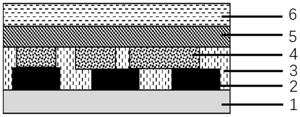
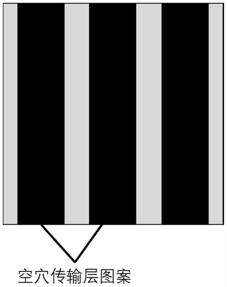
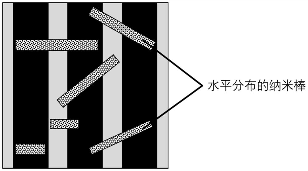
[0033] 40nm p-type GaN is epitaxially grown on a GaN substrate as a hole transport layer, and the p-type GaN layer is made into stripe patterns by photolithography, and nanometers with random horizontal orientation and flat end faces are grown on p-type GaN by CVD. The rods are used as resonators for laser emission. PMMA is spin-coated on the nanorod light-emitting layer as an insulating filling layer, and the PMMA covered on the top of the nanorods is removed by plasma treatment to make the nanorod light-emitting layer in good contact with the subsequently deposited electron transport layer. The electron transport layer was obtained by spin-coating a ZnO colloidal solution with a thickness of 30 nm. Finally, a LiF / Al electrode with a thickness of 1nm / 100nm was vapor-deposited as the cathode, and the nanorod electrolaser device was fabricated.
Embodiment 2
[0035] The p-type heavily doped Si is used as the conductive substrate and the hole transport layer, and the p-type region of the Si surface layer is made into a stripe pattern by photolithography. Phase growth method in situ grows nanorods with randomly distributed horizontal orientations and flat end faces as resonators for laser emission, and deposits 45nm Al on the luminescent layer of nanorods by ALD 2 O 3 As an insulating filling layer to ensure that the nanorod side regions are exposed for good contact with the subsequently deposited electron transport layer. The electron transport layer was deposited by thermal evaporation as TPBi with a thickness of 40 nm. Finally, a Ti / Au electrode with a thickness of 35nm / 100nm was vapor-deposited as the cathode, and the nanorod electro-laser device was fabricated.
Embodiment 3
[0037] ITO with a thickness of 120 nm was deposited on a glass substrate as a conductive substrate, and the ITO was fabricated into stripe patterns by photolithography with an etching depth of 40 nm, and PEDOT:PSS / TFB with a thickness of 40 nm / 20 nm was deposited on the ITO as a void Hole transport layer, nanorods with random distribution of long horizontal orientation and flat end faces are deposited on TFB by dry transfer as a resonator for laser emission, spin-coated PMMA on the nanorod light-emitting layer as an insulating filling layer, and treated by plasma Removing the PMMA covering the top of the nanorods made the nanorod light-emitting layer in good contact with the subsequently deposited electron transport layer. The electron transport layer was obtained by spin-coating a ZnO colloidal solution with a thickness of 30 nm. Finally, a LiF / Al electrode with a thickness of 1nm / 100nm was vapor-deposited as the cathode, and the nanorod electrolaser device was fabricated.
...
PUM
| Property | Measurement | Unit |
|---|---|---|
| thickness | aaaaa | aaaaa |
| thickness | aaaaa | aaaaa |
| thickness | aaaaa | aaaaa |
Abstract
Description
Claims
Application Information