

Method for preparing periodic microstructure on metallic film by femto second laser
A metal thin film and femtosecond laser technology, applied in optics, optical components, nonlinear optics, etc., can solve the problems of time-consuming, expensive, processing accuracy, processing quality, etc., and achieve the effect of simple preparation process and high efficiency
- Summary
- Abstract
- Description
- Claims
- Application Information
AI Technical Summary
Problems solved by technology
Method used
Image

Examples
Embodiment 1
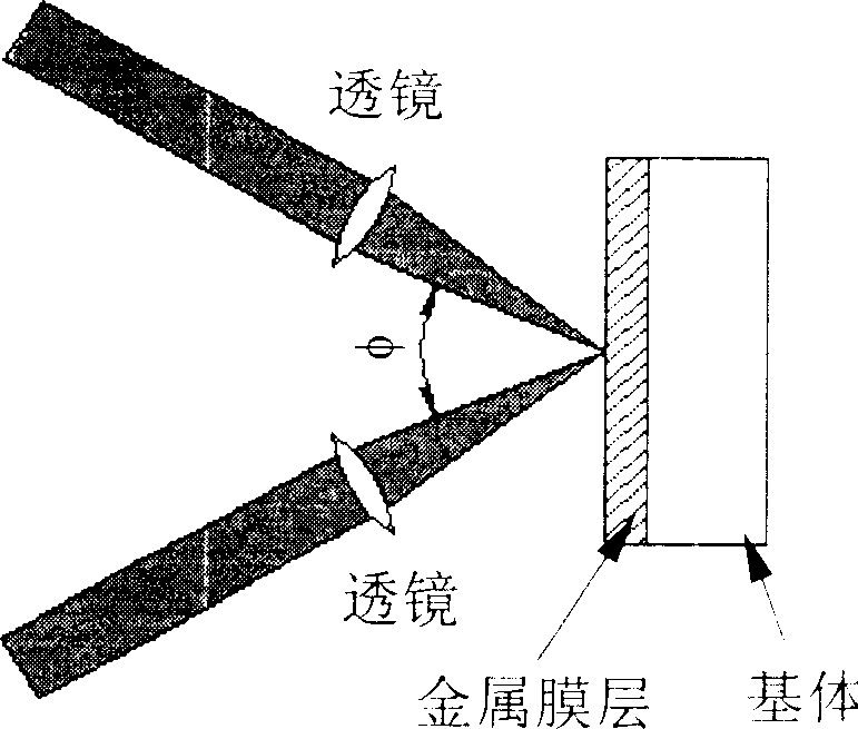
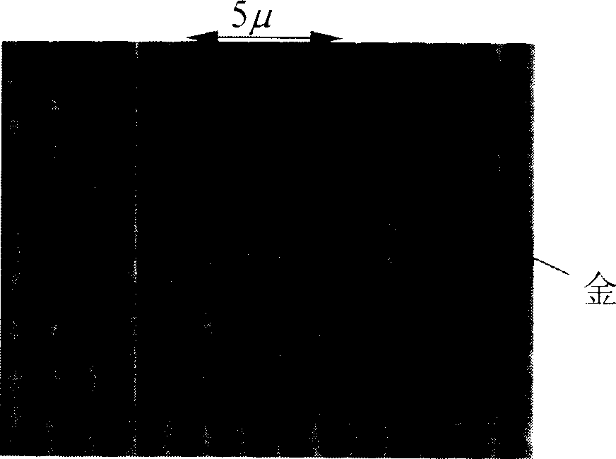
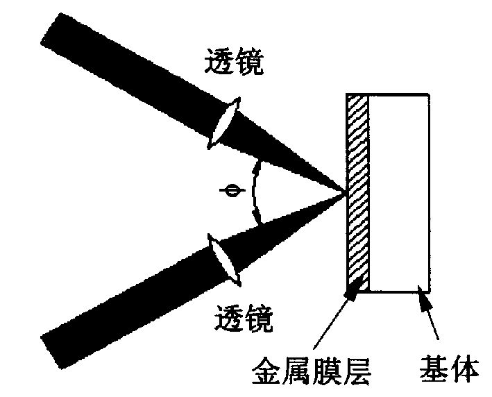
[0023] The femtosecond laser emitted by the titanium sapphire femtosecond laser is selected, the pulse width is 120fs, the wavelength is 800nm, the pulse frequency is 1Hz, and the pulse energy is 50μJ. The beam is divided into two beams at a ratio of 1:1 by a beam splitter. The diameter of the beam is 5mm, and the coherence of the two beams is realized by means of the second harmonic generated by the frequency-doubling crystal. The angle between the two beams is 40°, and the two beams are focused on the gold film Above, the sample is controlled by a computer-operated three-dimensional mobile platform, and the spot diameter at the focal point is about 40 μm. In this way, a periodic microstructure is formed in the laser coherence induction region. Using an optical microscope (100× / 0.9 objective lens) to focus on the laser-induced region in the glass sample, periodic microstructures such as figure 2 As shown, the structural period is 1.3 μm, and the gold film linearity is about...
Embodiment 2
[0025] Select a laser with a pulse width of 120 fs, a wavelength of 400 nm, a pulse frequency of 10 Hz, and a pulse energy of 50 μJ. The beam is divided into two beams with a ratio of 1:1 through a beam splitter. The beam diameter is 5 mm. The coherence of the two beams is achieved by The second harmonic generated by the frequency doubling crystal is realized. The angle between the two beams is 30°. Two focusing lenses with a focal length of 100mm are used to focus the two beams on the aluminum film. The sample is controlled by a three-dimensional mobile platform operated by a computer. The diameter of the spot at the focal point is about 40 μm. In this way, a periodic microstructure is formed in the laser coherence induction region. Using an optical microscope (100× / 0.9 objective lens) to focus on the laser-induced region in the glass sample, it was observed that the structural period was 1.5 μm, and the aluminum film line length was about 700 nm.
Embodiment 3
[0027] Choose a laser with a pulse width of 120 fs, a wavelength of 400 nm, a pulse frequency of 10 Hz, and a pulse energy of 50 μJ. The beam is divided into two beams at a ratio of 1:1 through a beam splitter. The beam diameter is 5 mm. The coherence of the two beams is achieved by means of The second harmonic generated by the frequency doubling crystal is realized. The angle between the two beams is 45°. Two focusing lenses with a focal length of 100mm are used to focus the two beams on the chromium film. The sample is controlled by a three-dimensional mobile platform operated by a computer. The diameter of the spot at the focal point is about 40 μm. In this way, a periodic microstructure is formed in the laser coherence induction region. Using an optical microscope (100× / 0.9 objective lens) to focus on the laser-induced region in the glass sample, it is observed that the structural period is 1.1 μm, and the chromium film linearity is about 500 nm.
PUM
| Property | Measurement | Unit |
|---|---|---|
| Thickness | aaaaa | aaaaa |
Abstract
Description
Claims
Application Information