
Piezoelectric element, ink-jet head, angular-rate sensor and its manufacturing method, ink-jet recorder

A piezoelectric element and piezoelectric layer technology, which is applied in the manufacture/assembly of piezoelectric/electrostrictive devices, electrical components, piezoelectric/electrostrictive/magnetostrictive devices, etc., can solve the problem of slow process PZT film , can not get an orientation film, crystal irregularity and other problems, to achieve the effect of reducing manufacturing costs

Inactive Publication Date: 2003-12-17
PANASONIC CORP
View PDF8 Cites 23 Cited by
  • Summary
  • Abstract
  • Description
  • Claims
  • Application Information

AI Technical Summary

Problems solved by technology

[0012] In addition, in the sol-gel method, since the film thickness of the PZT film formed in one step (coating of the precursor solution and subsequent heat treatment) is no more than about 100 nm at the most, it is necessary to obtain a piezoelectric element of 1 micron or more. film thickness, it is necessary to repeat the above process more than 10 times, so there will be a problem of low productivity
[0013] On the other hand, according to the aforementioned Japanese Unexamined Patent Publication No. 2001-88294, the sol-gel method (also known as the sol-gel method) is used as a method of temporarily forming an amorphous thin film, changing it into a crystalline thin film by post-processing such as heat treatment, and then synthesizing it. Methods other than the MOD method), that is, film-forming methods that directly form a crystalline thin film without using a heat-treated crystallization process, such as sputtering, laser polishing, and CVD, have attempted to provide an ultra-thin titanium layer on the surface of Ir Orientation control of PZT on the bottom electrode, but no alignment film can be obtained except for the sol-gel method
The reason is that, in the sol-gel method, the crystallization of the PZT film proceeds gradually from the lower electrode side to the upper electrode side, whereas in the CVD method, sputtering method, etc., the crystallization of the PZT film proceeds randomly, and the crystallization is irregular. sex, difficult to control orientation

Method used


Image

  • Piezoelectric element, ink-jet head, angular-rate sensor and its manufacturing method, ink-jet recorder
  • Piezoelectric element, ink-jet head, angular-rate sensor and its manufacturing method, ink-jet recorder
  • Piezoelectric element, ink-jet head, angular-rate sensor and its manufacturing method, ink-jet recorder

Examples


Embodiment 1

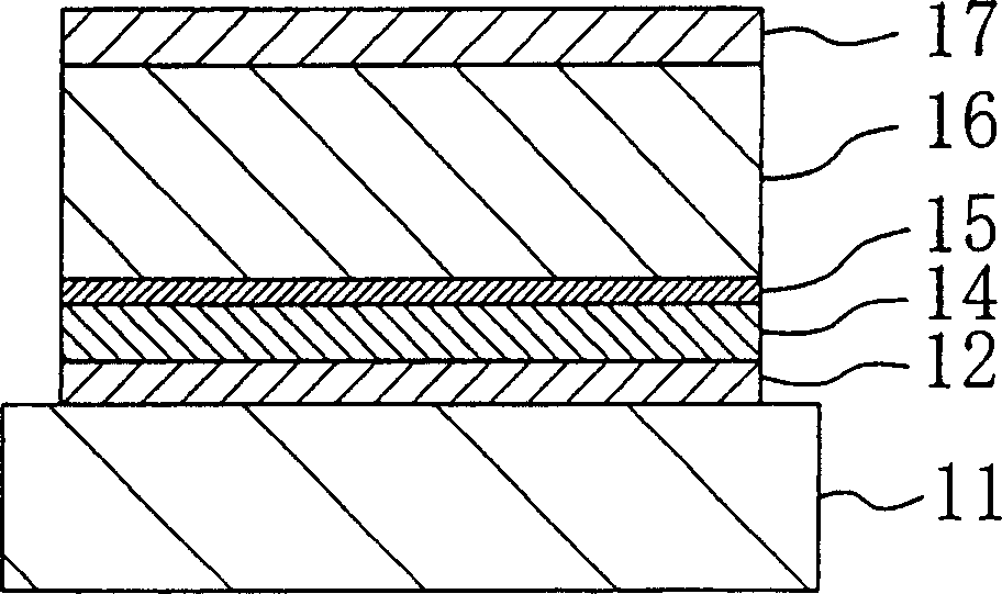
[0119] The material, film thickness, production method, etc. of each film in Example 1 are the same as those described in the above-mentioned embodiment. Cracks or film peeling were not seen in the respective films of the piezoelectric element of Example 1.

[0120] The crystal orientation and film composition of the piezoelectric layer before forming the second electrode layer were investigated. That is, according to the analysis by the X-ray diffraction method, the piezoelectric layer showed a (100) plane-oriented rhombohedral perovskite type crystal structure, and the (100) plane orientation degree was α=97%. In addition, as a result of composition analysis by an X-ray microanalyzer, the composition of the PZT film was the same as that of the target, and the Zr / Ti ratio was 53 / 47.

[0121] Next, the crystal orientation and film composition of the first electrode layer before forming the orientation control layer were studied. That is, as a result of analysis by the X-ray ...

Embodiment 2

[0126] In Example 2, the substrate is 0.25 mm thick and φ is 4 inches of stainless steel (SUS304), and a tantalum (Ta) film with a film thickness of 0.01 micron is used in the adhesion layer, and a film thickness of 0.01 micron is used in the first electrode layer. 0.25 micron Pt film containing 9 mol% of strontium oxide, 0.03 micron in film thickness, containing 17 mol% of lanthanum and 10 mol% of zirconium in the orientation control layer, and the lead content is excessive compared with the stoichiometric theoretical composition For the 6 mol% PLZT film, a PZT film (Zr / Ti=40 / 60) with a film thickness of 2.8 microns was used for the piezoelectric layer, and a Pt film with a film thickness of 0.1 micron was used for the second electrode layer.

[0127] Using a Ta target, the substrate was heated to 500° C. and a high-frequency power of 100 W was applied, and formed in an argon gas of 1 Pa for 1 minute to obtain the above-mentioned adhesion layer.

[0128] Using a Pt alloy targ...

Embodiment 3

[0139]In Example 3, the substrate is barium borosilicate glass (100 mm square size) with a thickness of 0.5 mm, and a nickel (Ni) film with a film thickness of 0.005 microns is used for the adhesion layer, and a film of nickel (Ni) is used for the first electrode layer. A 0.15 micron thick iridium (Ir) film containing 18 mol% Ca was used in the orientation control layer. The orientation control layer was made of strontium titanate containing 18 mol% Sr and 15 mol% Zr with a lead content equal to A film composed of a solid solution of PZT with an excess of 16 mol% of the stoichiometric composition, a PZT film (Zr / Ti=60 / 40) with a film thickness of 2.5 microns is used for the piezoelectric layer, and a PZT film (Zr / Ti=60 / 40) is used for the second electrode layer Pt film with a film thickness of 0.01 µm.

[0140] Using a Ni target, the substrate was heated to 300° C., and a high-frequency power of 200 W was applied, and formed in an argon gas of 1 Pa for 1 minute to obtain the a...


PUM

PropertyMeasurementUnit
coating thicknessaaaaaaaaaa

Abstract

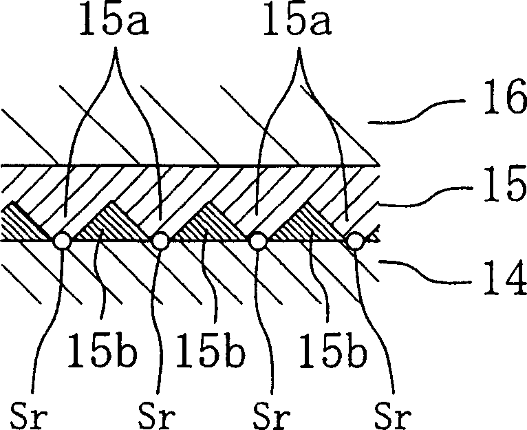
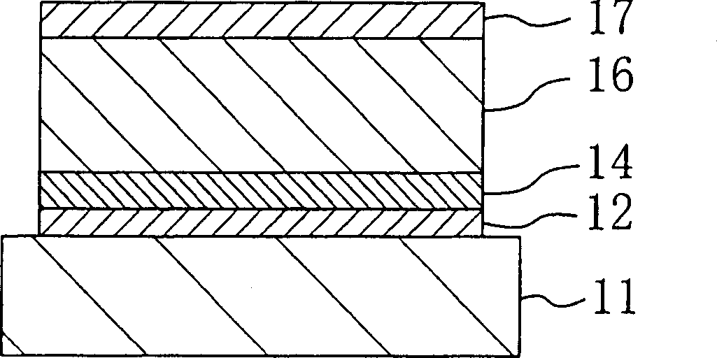
A piezoelectric element includes a first electrode layer 14 provided on a substrate 11 and made of a noble metal to which at least one additive selected from the group consisting of Mg, Ca, Sr, Ba, Al and oxides thereof is added, an orientation control layer 15 provided on the first electrode layer 14 and made of a cubic or tetragonal perovskite oxide that is preferentially oriented along a (100) or (001) plane, and a piezoelectric layer 16 provided on the orientation control layer 15 and made of a rhombohedral or tetragonal perovskite oxide that is preferentially oriented along a (001) plane.

Description

technical field [0001] The present invention relates to a piezoelectric element exhibiting an electromechanical conversion function, an inkjet head using the piezoelectric element, an angular velocity sensor and a manufacturing method thereof, and an inkjet type recording apparatus equipped with the above inkjet head as a printing apparatus. Background technique [0002] In general, a piezoelectric material is a material that converts mechanical energy into electrical energy, or converts electrical energy into mechanical energy. As a representative of the piezoelectric material, lead zirconate titanate (Pb(Zr,Ti)O 3 ) (hereinafter referred to as PZT). In this PZT, the direction in which the maximum piezoelectric displacement is obtained is the <001> direction (c-axis direction) in the case of the tetragonal crystal system, and the <111> direction in the case of the rhombohedral crystal system. However, since most piezoelectric materials are polycrystals compose...

Claims


Application Information

Patent Timeline
Patent Type & Authority Applications(China)
IPC IPC(8): B41J2/14B41J2/16G01C19/5607H01L41/047H01L41/22H01L41/24
CPCB41J2/1632B41J2/1628H01L41/047G01C19/5607B41J2/1645B41J2/161B41J2/1623H01L41/316B41J2/1646B41J2002/14491H01L41/1876B41J2/1642B41J2/1631B41J2/14233H10N30/877H10N30/8554H10N30/076H10N30/708
Inventor 友泽淳藤井映志鸟井秀雄村田晶子高山良一平泽拓
Owner PANASONIC CORP
Learn More