Method for processing beam, laser irradiating apparatus and method for manufacturing semiconductor device

A technology of semiconductors and lasers, which is applied in the direction of semiconductor devices, semiconductor/solid-state device manufacturing, laser components, etc., to achieve the effects of reduced manufacturing costs, high working characteristics, and improved energy distribution uniformity

Inactive Publication Date: 2010-04-28
SEMICON ENERGY LAB CO LTD
View PDF5 Cites 0 Cited by
  • Summary
  • Abstract
  • Description
  • Claims
  • Application Information

AI Technical Summary

Problems solved by technology

[0024] Another problem with YAG lasers involves the coherence of YAG lasers

Method used


Image

  • Method for processing beam, laser irradiating apparatus and method for manufacturing semiconductor device
  • Method for processing beam, laser irradiating apparatus and method for manufacturing semiconductor device
  • Method for processing beam, laser irradiating apparatus and method for manufacturing semiconductor device

Examples


Embodiment 1

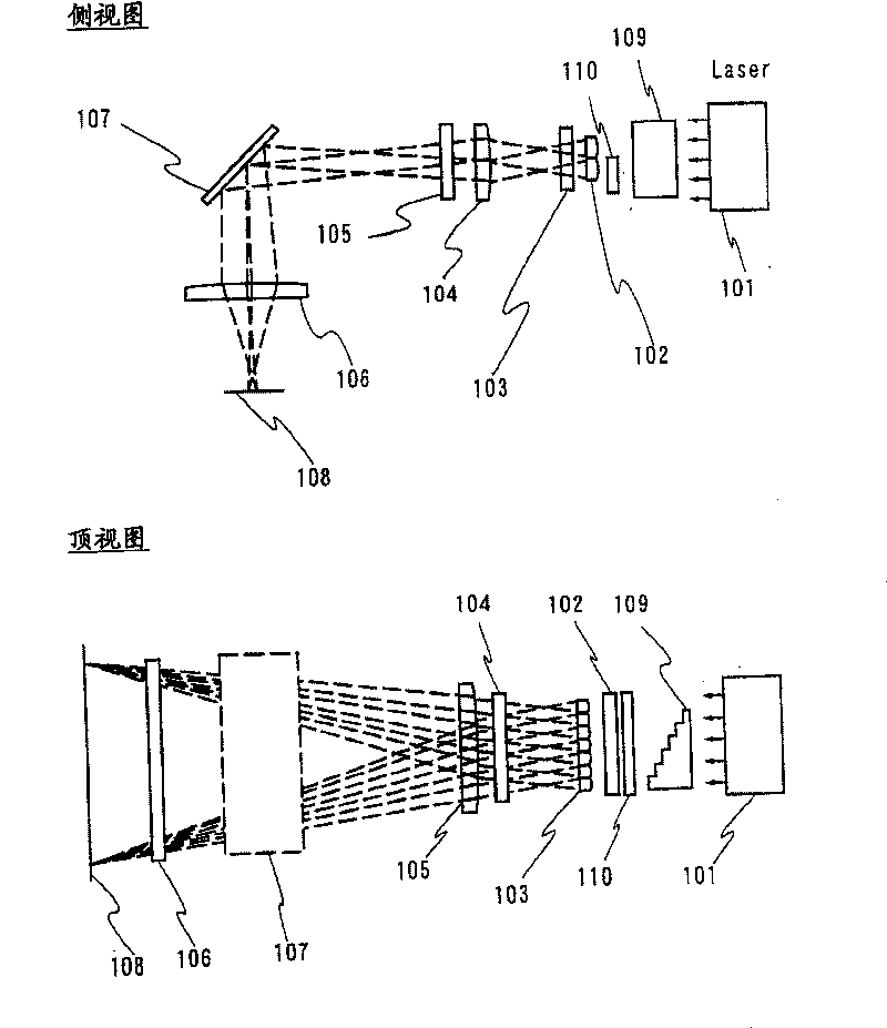
[0073] A first embodiment of the present invention will be described below with respect to a manufacturing process of a semiconductor device in which an amorphous silicon film is formed on a glass substrate and crystallized by the laser irradiation method of the present invention.

[0074] First, an example of a method of forming an amorphous silicon film will be described. A 5 inch square Corning 1737 substrate was first cleaned to remove foreign particles on the substrate surface. Then, a 100 nm-thick silicon nitride oxide film and a 55 nm-thick amorphous silicon film were formed on the substrate by a plasma CVD apparatus. The silicon oxynitride film referred to in this specification is an insulating material film represented by SiOxNy, that is, an insulating film containing silicon, oxygen, and nitrogen in predetermined proportions. Amorphous silicon films may contain a considerable amount of hydrogen. In this case, the laser resistance of the amorphous silicon film is im...

Embodiment 2

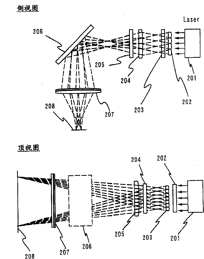
[0086]Next, a second embodiment of the present invention will be described with respect to irradiating a semiconductor polycrystalline film with a line beam to perform an annealing process.

[0087] First, a method of forming a polycrystalline semiconductor will be described. A 5 inch Corning 1737 substrate was first cleaned to remove foreign particles from the substrate surface. Then, a 100nm-thick silicon nitride oxide film and a 55nm-thick amorphous silicon film were formed on the substrate by a plasma CVD device. The silicon oxynitride film referred to in this specification is an insulating material film represented by SiOxNy, that is, an insulating film containing silicon, oxygen, and nitrogen in predetermined proportions. Next, the amorphous silicon film is processed by a method such as that described in Japanese Patent Application Laid-Open No. Hei 7-183540. That is, an aqueous solution of nickel acetate (5 ppm by weight, 5 ml in volume) was applied to the surface of ...

Embodiment 3

[0091] see Figure 5 , shows an example of a laser irradiation device for mass production in the third embodiment. Figure 5 is a top view of the laser irradiation device.

[0092] The substrate is transported from the load / unload chamber 1501 using the robot arm 1503 for transport installed in the transport chamber 1502 . First, after the substrate is positioned in the alignment chamber 1504, it is transported to the preheating chamber 1505. The temperature of the substrate is then heated in advance to a desired temperature, for example about 300° C., using a heater such as an infrared lamp. After that, the substrate is fixedly placed in the laser irradiation chamber 507 passing through the gate valve 1506 . Then the gate valve 1506 is closed, and the temperature of the substrate is increased to compensate for the lack of energy of the laser beam. Especially in cases where processing large area substrates requires extended line beam lengths, the laser energy can be contro...


PUM

PropertyMeasurementUnit
strain pointaaaaaaaaaa
thicknessaaaaaaaaaa
thicknessaaaaaaaaaa

Abstract

PROBLEM TO BE SOLVED: To solve the problem of an excimer laser being used frequently in laser annealing of a non-single crystal semiconductor film, a solid-state laser such as a YAG laser or the likebeing easy in inspection and maintenance of a laser body, as compared with excimer laser, and when this becomes another as a substitute for the excimer laser, its cost can be reduced but since the solid-state laser is heretofore tends relatively to interfere with the laser beam, so that a method for simply dividing and combining the beam to make the energy uniform cannot be used. SOLUTION: The laser beams in the solid-state laser can be laser oscillated, by aligning polarizing surfaces. A method for processing with the laser beam comprises the steps of forming the two laser beams of independentpolarization directions by a &lambda / 2 plate 110; further forming a plurality of laser beams having different optical path lengths by a stepwise quartz plate 109, and combining the beams at thei rradiating surface 108 or its vicinity to one by an optical system to make the beam uniform. Thus, the beam, in which interference is very mach suppressed, and the uniformity of the energy is high,is obtained.

Description

[0001] This application is a divisional application of an invention patent application with the filing date of September 1, 2001, the application number of 01135754.1, and the title of the invention entitled "Method for Processing Light Beam, Laser Irradiating Device, and Method for Manufacturing Semiconductor Devices". technical field [0002] The present invention relates to a method for uniformly distributing the energy of a laser beam in a specific area, and to a laser irradiation device (including a laser device and a laser device output The laser beam guides the target optical system). The invention also relates to a method of manufacturing a semiconductor device by a process comprising laser annealing. In this specification, "semiconductor device" means any kind of device capable of functioning by utilizing semiconductor characteristics, including electro-optical devices such as liquid crystal display devices and electroluminescence (EL) displays, and also including ele...

Claims


Application Information

Patent Timeline
Patent Type & Authority Patents(China)
IPC IPC(8): H01L21/324H01L21/20H01L21/00G02F1/01G02F1/35B23K26/00H01S3/10B23K26/06B23K26/067B23K26/073G02B27/09G02B27/10
CPCG02B27/0961G02B27/149B23K26/0608G02B27/0966B23K26/067G02B27/145G02B27/09G02B27/0905G02B27/123B23K26/0604B23K2201/40B23K26/073B23K2101/40H01S3/10
Inventor 田中幸一郎
Owner SEMICON ENERGY LAB CO LTD
Why Eureka
Try Eureka