Vertical double diffusion metal oxide semiconductor power device

An oxide semiconductor, vertical double diffusion technology, applied in the direction of semiconductor devices, electrical components, circuits, etc., can solve the problem that the ability to resist radiation cannot be fully improved, the ability to resist single particle radiation is weakened, and the surface utilization of silicon wafers is not good. For advanced problems, the effect of increasing the single event failure threshold, improving the anti-radiation ability, and improving the anti-transient irradiation ability

Inactive Publication Date: 2006-08-23
UNIV OF ELECTRONIC SCI & TECH OF CHINA
View PDF0 Cites 6 Cited by
  • Summary
  • Abstract
  • Description
  • Claims
  • Application Information

AI Technical Summary

Problems solved by technology

The structure improves the radiation resistance of the device by introducing a part of the buried oxide layer with high electron-hole pair recombination ability, but the device is affected by the floating body effect, and its resistance to single-particle radiation is weakened, so its

Method used


Image

  • Vertical double diffusion metal oxide semiconductor power device
  • Vertical double diffusion metal oxide semiconductor power device
  • Vertical double diffusion metal oxide semiconductor power device

Examples


Embodiment Construction

[0050] By adopting the partially buried oxygen structure of the present invention, a radiation-resistant, high-voltage, high-speed power device with excellent performance can be obtained. It can be applied to common power devices such as double diffused field effect transistors, insulated gate bipolar power transistors, static induced transistors, and PN diodes. Devices with a partially buried oxygen structure can be used in aerospace, nuclear environment, and other fields that require higher device resistance to radiation. With the development of semiconductor technology, more radiation-resistant, high-voltage, and high-speed power devices can be manufactured by using the present invention.

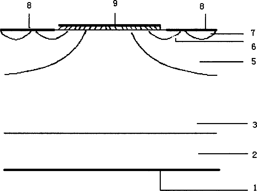
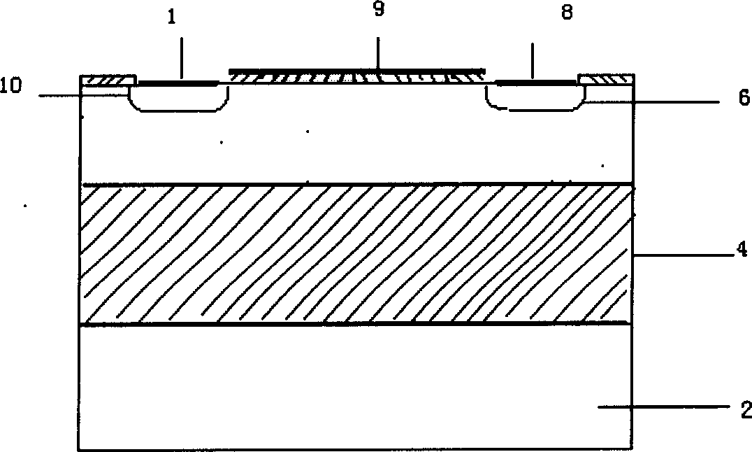
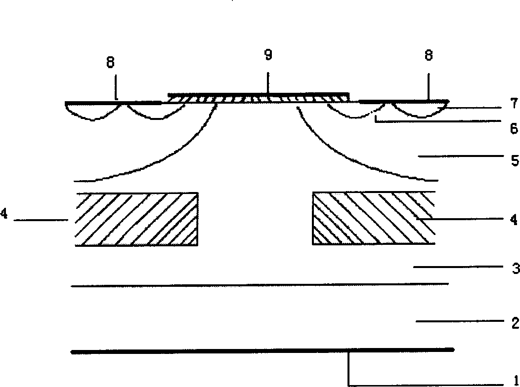
[0051] Introduce a new type of vertical DMOS power device with a partially buried oxygen structure, such as figure 2 Shown, including drain 1, n + (Or p + ) Substrate area 2, n - (Or p - ) Epitaxial layer 3, p (or n) region 5, n + (Or p + ) District 6, p + (Or n + ) District 7, source 8, ga...


PUM


Abstract

A vertical double diffusion MOS power device belongs to semiconductor power device technology field. Present invention leads in part oxygen burying zone located both sides of device main vertical electrically conductive paths, said oxygen burying zone capable of being done on epitaxial layer, or simultaneously occupying substrate and part area of epitaxial layer, or simultaneously occupying epitaxial layer and P/N zone part area, also occupying simultaneously substrate, epitaxial layer and P/N zone part area, its shape capable of being rectangular, trapezia and ellipse etc, made from silicon dioxide or silicon nitride etc insulating material. Present invention raises voltage withstand and anti irradiation ability through part oxygen burying structure provided high voltage withstand, high electronic-hole pair recombination compound channel. Compared with traditional vertical DMOS, under same conduction resistance, said invention raises voltage withstand by more than 20 per cent, transient state irradiation ability by more than two times, and single particle fault threshold by almost one times. Present invention can make different kinds of high-speed vertical DMOS device with fine anti irradiation and high voltage performance.

Description

Technical field [0001] A vertical double diffused metal oxide semiconductor power device belongs to the technical field of semiconductor power devices. Background technique [0002] Vertical double diffused metal oxide semiconductor (V-DMOS) compared to the earlier horizontal DMOS, it transfers the drain region, drift region, and channel region from the surface to the bottom and body of the silicon wafer, respectively. The die occupies The silicon wafer area has been greatly reduced, the utilization rate of the silicon wafer surface has been improved, and the frequency characteristics of the device have also been greatly improved, making the power MOS device a big step forward in the process of moving from low power to high power. Vertical DMOS is suitable for making high-power devices and is an important basis for power electronics. As a power switch, vertical DMOS devices are often used in power integrated circuits and power integrated systems due to their high withstand voltag...

Claims


Application Information

Patent Timeline
IPC IPC(8): H01L29/78
Inventor 李泽宏张子澈张磊易黎张波李肇基
Owner UNIV OF ELECTRONIC SCI & TECH OF CHINA
Why Eureka
Try Eureka