Method for producing flexible printed wiring board, and flexible printed wiring board

A flexible printing and manufacturing method technology, applied in the direction of printed circuit manufacturing, printed circuit, printed circuit components, etc., can solve problems such as wiring short circuit, pattern compression, poor contact of IC chip connection, etc., and achieve the effect of high-precision connection

Inactive Publication Date: 2006-10-04
MITSUI MINING & SMELTING CO LTD
View PDF3 Cites 18 Cited by
  • Summary
  • Abstract
  • Description
  • Claims
  • Application Information

AI Technical Summary

Problems solved by technology

[0008] However, in this method, when the pitch is high, such as 30 μm, the width of the bottom of the wiring is 15 μm, and the width of the top is 12 μm, and an opening with a diameter of 10 μm is formed thereon and copper is electroplated. , or the height deviation of the bumps, there is a problem of bad contact when connecting with the IC chip
Moreover, due to the cross-sectional shape of the film after development, the bump tends to become a rounded truncated shape, and there is a problem that stress concentration occurs on the flexible printed circuit board during bonding and the pattern is too compressed.
In addition, when copper is electroplated, copper may adhere to the side surface of the wiring, and there is a problem of short-circuiting with adjacent wiring.
Moreover, in this method, there is also the problem that the resist setting process and the exposure and development process must be performed twice.

Method used


Image

  • Method for producing flexible printed wiring board, and flexible printed wiring board
  • Method for producing flexible printed wiring board, and flexible printed wiring board
  • Method for producing flexible printed wiring board, and flexible printed wiring board

Examples


Embodiment 1

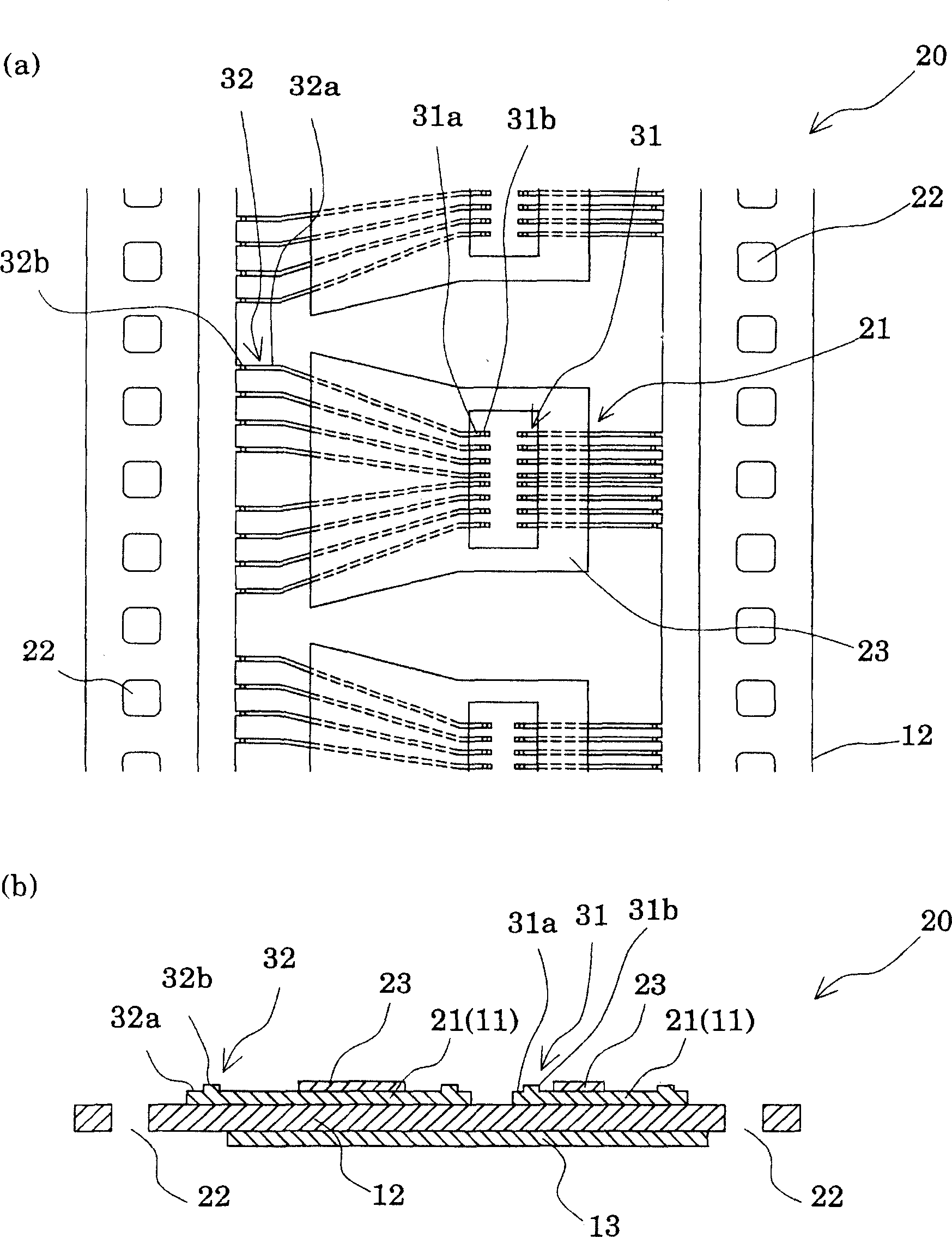
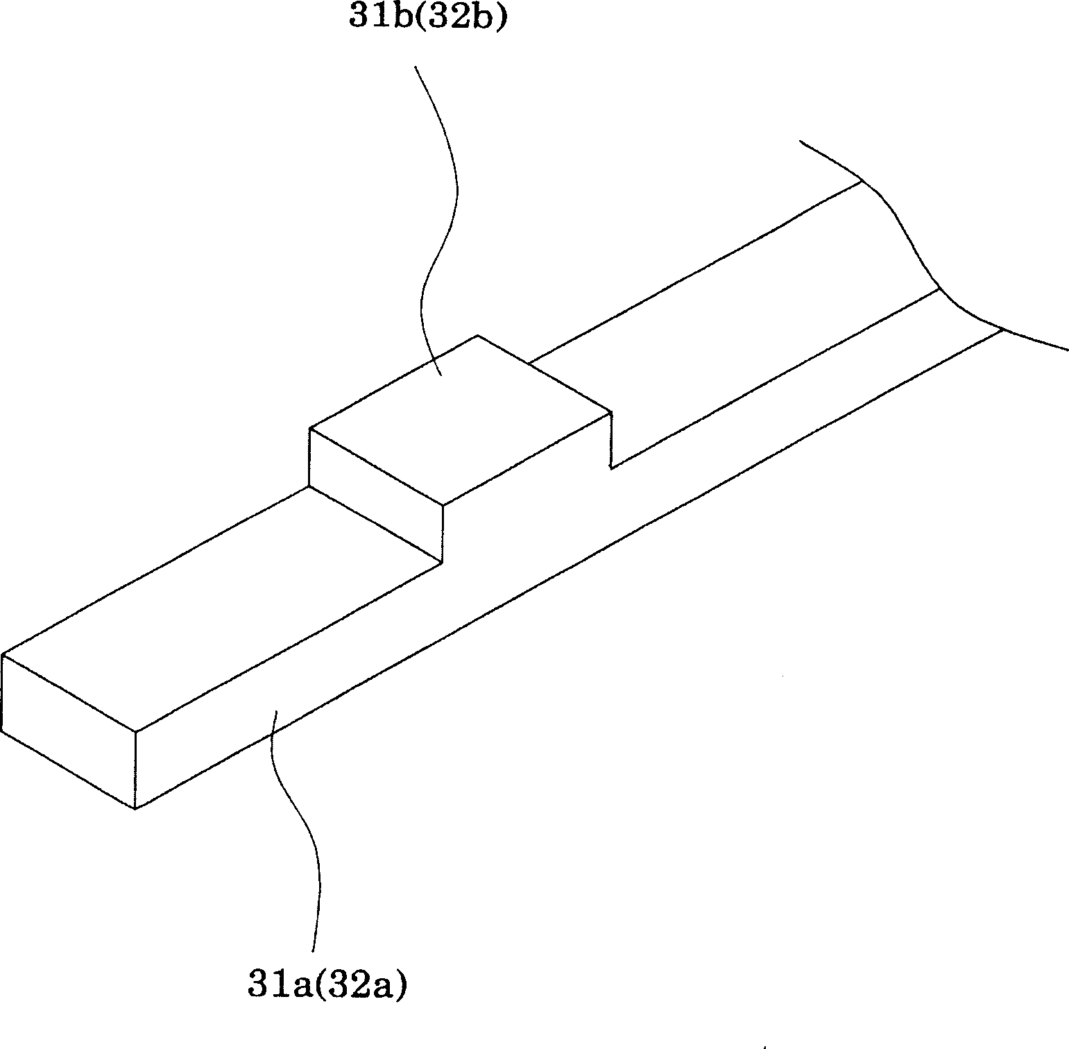
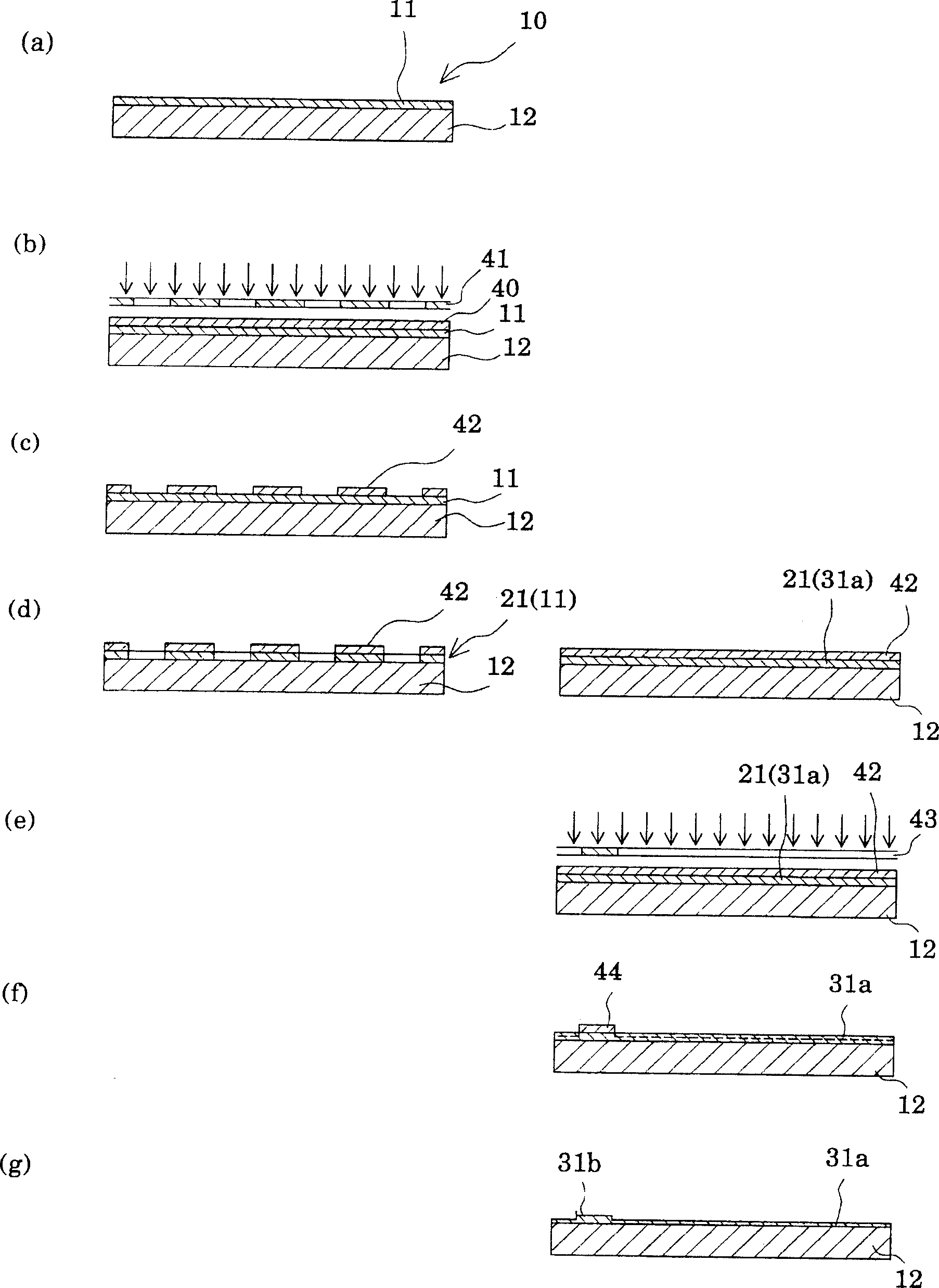
[0081] To the copper foil side of a laminated film (Espanex M, manufactured by Nippon Steel Chemical Co., Ltd.) formed by laminating a copper foil with a thickness of 12 μm on a polyimide film with a thickness of 40 μm, a thickness of 30 cps with a viscosity Roll-coat positive type liquid photoresist FR200 (manufactured by Rohm & Haas Co.) on the entire surface in a 4-5 μm manner, and after drying, form a prescribed wiring circuit pattern (in this example, as an external lead , including 720 linear wirings with a width of 35 μm arranged side by side at a pitch of 50 μm), a glass photomask for ultraviolet light (320mJ / cm 2 ) is exposed to light.

[0082] Then, a photoresist pattern is formed by developing, and the solution of divalent copper chloride+hydrochloric acid+hydrogen peroxide is sprayed at 1.2kg / cm 2continuous etching. After etching, it is pickled with hydrochloric acid and then washed with water to obtain a wiring pattern including external leads. At this time, th...

Embodiment 2

[0087] In this embodiment, nodules in the shape of nodules or needles are formed on the bumps to improve connectivity with the LCD substrate or the like.

[0088] In this embodiment, a laminated film (Espanex M, manufactured by Nippon Steel Chemical Co., Ltd.) formed by laminating copper foil with a thickness of 15 μm on a polyimide film with a thickness of 40 μm is used, and the implementation is the same as in Example 1. The steps up to the etching step to form bumps are the same as those in Embodiment 1, and therefore description thereof will be omitted.

[0089] After the etching step is completed, a solder resist coating solution is printed onto the outer leads and portions other than the inner leads.

[0090] Then, in a plating bath prepared by adding 50 ppm of β-naphthoquinone to a copper sulfate solution (Cu: 8gr / L, sulfuric acid: 100gr / L), Dk = 3A / dm at 30°C 2 Plating for 15 seconds at 1A / dm 2 In the usual precipitation state, copper plating is performed to fix the ...


PUM


Abstract

The present invention provides a method for producing a flexible printed wiring board which allows formation of a bump on a wire trace even in a high-density mounting process, and a flexible printed wiring board which realizes high-density mounting with high reliability. In the method for producing a flexible printed wiring board including an insulating layer and a wiring pattern on which a semiconductor chip is to be mounted, the pattern being formed of a conductor layer provided on at least one surface of the insulating layer, the method includes a first etching step including applying a photoresist onto a conductor layer and light-exposing the photoresist by the mediation of a first mask, followed by development, to thereby form a first resist pattern, and etching the conductor layer so as to penetrate the layer in the depth direction, to thereby form a first wiring pattern; and a second etching step including light-exposing the first resist pattern by the mediation of a second mask, followed by development, to thereby form a second resist pattern formed of a remaining portion of the first resist pattern, subsequently, leaving, as a thick portion, a portion of the first wiring pattern covered by the second resist pattern, and half-etching a portion other than the thick portion to an intermediate thickness of the conductor layer, to thereby form a second wiring pattern in the form of a thin portion having a thickness relatively smaller than that of the thick portion.

Description

technical field [0001] The present invention relates to a method for manufacturing flexible printed wiring boards such as film carrier tapes for COFs, flexible printed circuits (FPCs) for COFs, etc. suitable for mounting electronic components such as ICs and LSIs, and flexible printed wiring boards. Background technique [0002] With the development of the electronics industry, the demand for printed circuit boards for mounting electronic components such as IC (Integrated Circuit) and LSI (Large-Scale Integration) has increased rapidly, but miniaturization, weight reduction, and high functionality of electronic equipment are required. As the mounting method of the above-mentioned electronic components, the use of film carrier tapes for mounting electronic components such as TAB (Tape Automated Bonding) tape, T-BGA (Ball Grid Array), TAB tape for ASIC, and FPC (flexible printed circuit) has recently been adopted. Way. In particular, it is becoming more and more important in ...

Claims


Application Information

Patent Timeline
Patent Type & Authority Applications(China)
IPC IPC(8): H01L21/48H01L21/60H01L23/498H01L23/12H05K1/02H05K3/06
CPCH05K3/06H01L2924/3011H05K2203/1476H05K2203/0369H01L23/4985H05K3/4007H01L2924/0002H01L2924/00G07F17/0064G07F13/04
Inventor 河村裕和
Owner MITSUI MINING & SMELTING CO LTD
Why Eureka
Try Eureka