Prepn process of nanometer silicon line array

A silicon nanowire array and silicon wafer surface technology, applied in nanostructure manufacturing, nanotechnology, nanotechnology, etc., can solve problems such as difficulty in obtaining uniformly arranged nanowires in diameter, and difficulty in controlling the diameter of silicon wires. The effect of orderly layout, low cost and simple process

Inactive Publication Date: 2007-01-03
TSINGHUA UNIV
View PDF1 Cites 25 Cited by
  • Summary
  • Abstract
  • Description
  • Claims
  • Application Information

AI Technical Summary

Problems solved by technology

The method of pre-depositing catalyst particles and then growing nanowires has attracted much attention in recent years, but it is difficult to control the diameter of silicon wires in this preparation method
Chinese patent [CN 1382626A] proposes a method for preparing silicon nanowire...

Method used


Image

  • Prepn process of nanometer silicon line array
  • Prepn process of nanometer silicon line array

Examples


Embodiment 1

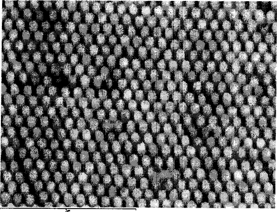
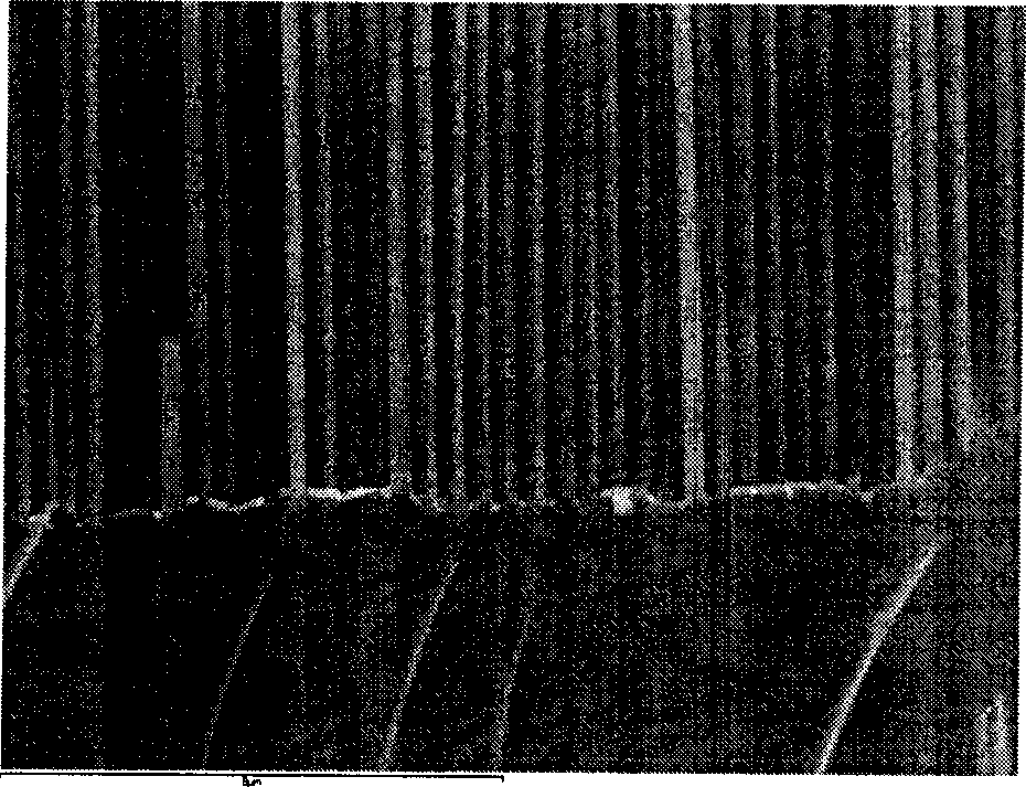
[0027] According to the surface area of ​​the substrate, the solution of polystyrene beads with a concentration of 0.01% was dropped onto the surface of the cleaned silicon wafer, dried and kept at 90° C. for 6 minutes. Perform reactive ion etching on the PS balls for 60 ± 5 seconds, and then use a vacuum evaporation device to vapor-deposit a 25nm (± 3nm) thick Ag film on the surface of the silicon wafer where the PS ball array is arranged, and then deposit a silver film The sample was immersed in a closed container kettle containing a mixed solution of hydrofluoric acid and hydrogen peroxide (the concentrations of hydrofluoric acid and hydrogen peroxide were 1.15mol / L and 0.44mol / L respectively) and treated for 10 minutes, and a large area of ​​organic matter could be obtained. array of silicon nanowires.

Embodiment 2

[0029] According to the surface area of ​​the substrate, the solution of polystyrene beads with a concentration of 0.09% was dropped onto the surface of the cleaned silicon wafer, dried and kept at 90° C. for 10 minutes. Perform reactive ion etching on the PS balls for 80±5 seconds, and then use a vacuum evaporation device to vapor-deposit a 40nm (±5nm) thick Ag film on the surface of the silicon wafer where the PS ball array is arranged, and then deposit a silver film The sample was immersed in a closed container kettle containing a mixed solution of hydrofluoric acid and hydrogen peroxide (the concentrations of hydrofluoric acid and hydrogen peroxide were 2.3mol / L and 0.88mol / L respectively) and treated for 30 minutes, and a large area of ​​organic matter could be obtained. array of silicon nanowires.

Embodiment 3

[0031] According to the surface area of ​​the substrate, the solution of polystyrene beads with a concentration of 0.1% was dropped onto the surface of the cleaned silicon wafer, dried and kept at 100° C. for 20 minutes. Perform reactive ion etching on the PS balls for 120 ± 5 seconds, and then use a vacuum evaporation device to vapor-deposit a 40nm (± 5nm) thick Ag film on the surface of the silicon wafer where the PS ball array is arranged, and then deposit a silver film The sample was immersed in a closed container kettle containing a mixed solution of hydrofluoric acid and hydrogen peroxide (the concentrations of hydrofluoric acid and hydrogen peroxide were 2.3mol / L and 1.76mol / L respectively) and treated for 20 minutes, and a large area of ​​organic matter could be obtained. array of silicon nanowires.


PUM


Abstract

The present invention is preparation process of nanometer silicon line array, and belongs to the field of nanometer material preparing technology. The preparation process includes the following steps: washing silicon chip successively with acetone, alcohol, acid cleaning solution and No. 1 standard washing solution; dropping 0.01-0.9 wt% concentration polyethylene pellet solution to the surface of silicon chip and drying in the air; etching the silicon chip with reaction ion in oxygen atmosphere for 1-2 min, maintaining at 90-110 deg.c for 1-6 min, depositing 25-50 nm thick Ag film with vacuum deposition instrument; and soaking the deposited sample inside the etching solution of hydrofluoric acid and hydrogen peroxide for 4-30 min. The preparation process can prepare great area ordered arranged nanometer silicon line array, and is simple, low in cost and suitable for large scale production.

Description

technical field [0001] The invention relates to a method for preparing a silicon nanowire array, in particular to a method for preparing a silicon nanowire array with a large area diameter, uniform length, and orderly arrangement, and belongs to the technical field of nanomaterial preparation and application. Background technique [0002] Semiconductor nanowires show promising applications in electronics and optics. Silicon is the most important material in today's semiconductor industry, and silicon nanowires have attracted researchers' attention because of their excellent properties and good process compatibility. In the process of deviceization of silicon-based nanomaterials, it has always been an important challenge to precisely control the size, crystallographic orientation, position, and arrangement of silicon-based nanomaterials. There are several main ways to control the size and combination of silicon-based nanomaterials: through photolithography, electron beam (E-...

Claims


Application Information

Patent Timeline
IPC IPC(8): B82B1/00
Inventor 黄智鹏朱静
Owner TSINGHUA UNIV
Why Eureka
Try Eureka