Light filtering plate with function of preventing electromagnetic radiation and filtering light for plasma display
An anti-electromagnetic radiation and plasma technology, applied in gas discharge tubes/containers, instruments, circuits, etc., can solve the difficulty of controlling film thickness and visible light transmittance, reduce the EMI shielding ability of three-layer silver, and the EMI shielding effect is not enough, etc. problems, to achieve the effect of low cost, increased convenience and long service life
- Summary
- Abstract
- Description
- Claims
- Application Information
AI Technical Summary
Problems solved by technology
Method used
Image
Examples
Embodiment 1
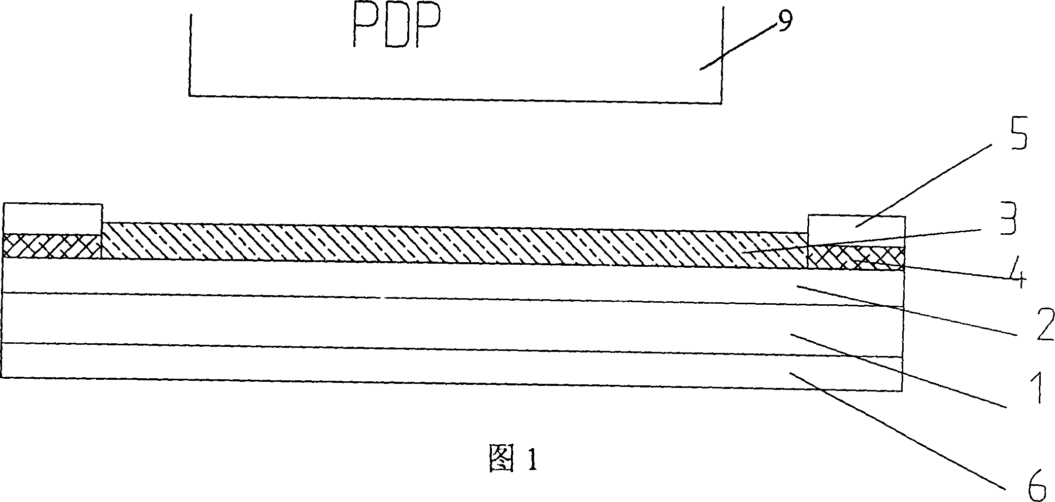
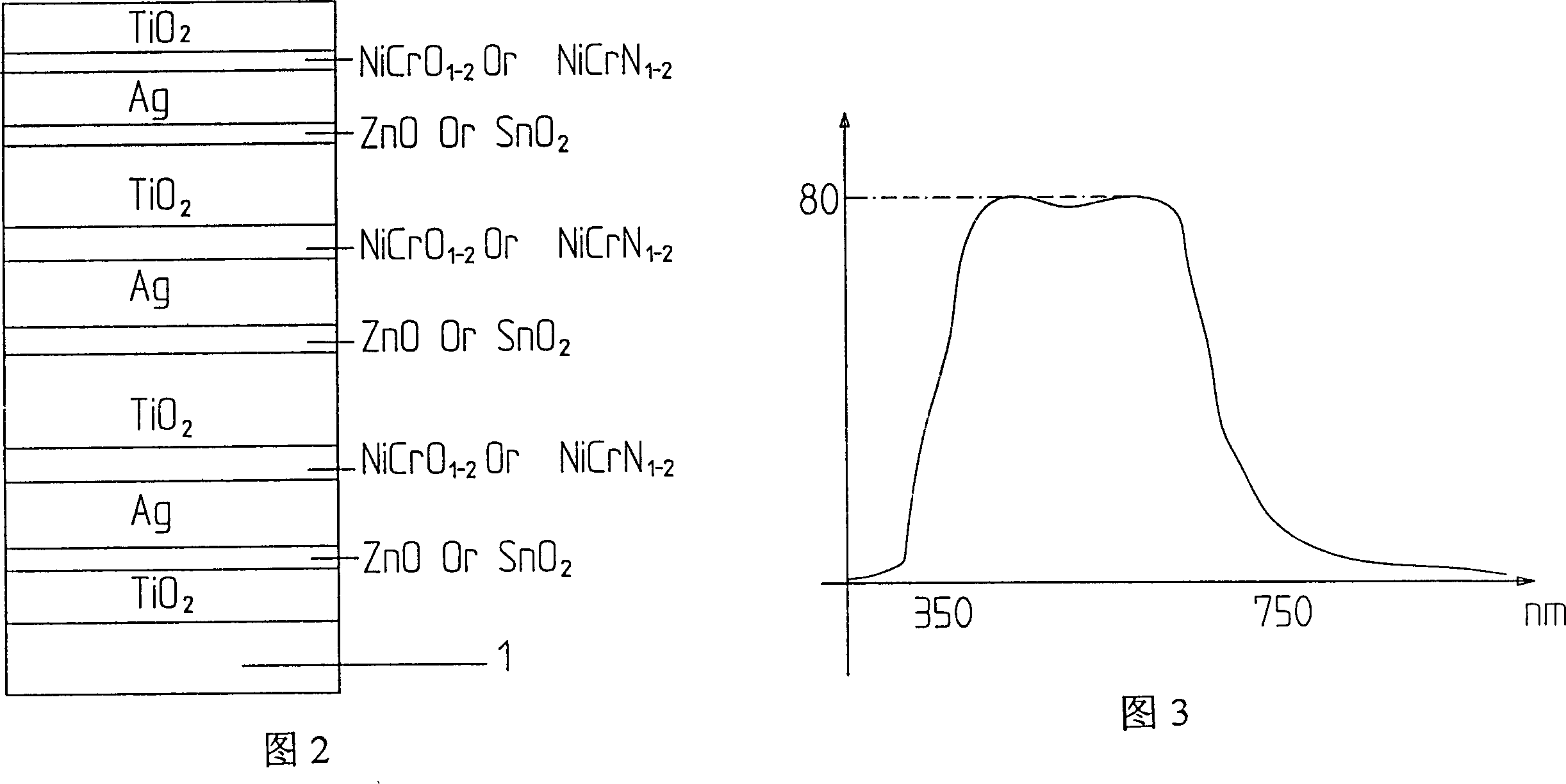
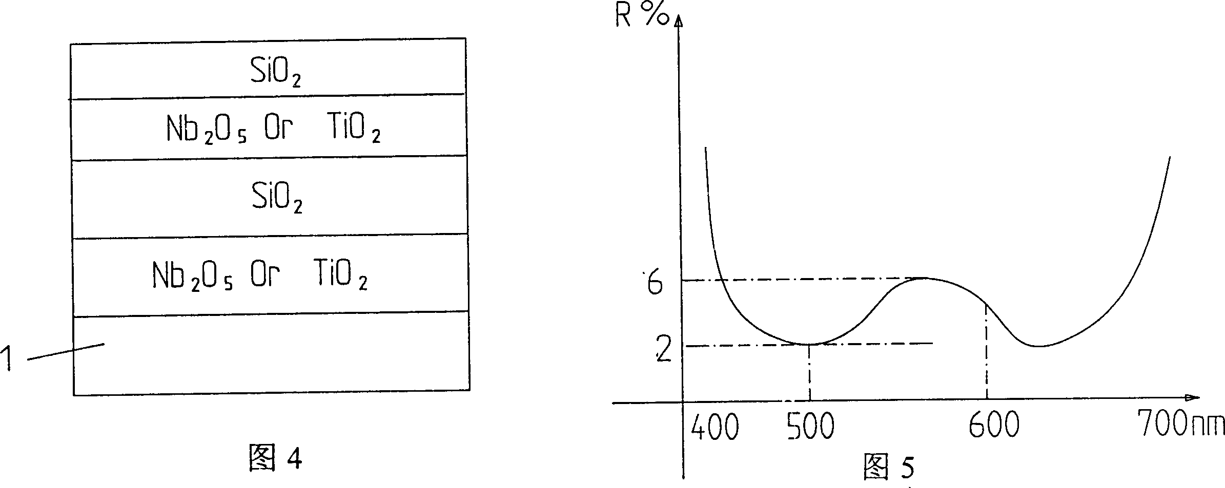
[0026] Figure 1 shows the first diagram of this embodiment. Referring to Figure 1, the substrate 1 is made of 3mm thick optical grade float glass (temperable) or 2mm thick polymethyl methacrylate (PMMA) plastic substrate or 0.2mm thick polyester (PET) substrate, After cleaning with deionized water, it enters the continuous magnetron sputtering coating production line and uses continuous magnetron sputtering to coat the three-silver film system (or four-silver film system) as shown in Figure 2. 2 / ZnO (or SnO 2 ) / Ag / NiCrOx(or NiCrNx) / TiO 2 13-layer film composed of repeating structures (adjacent TiO layers of adjacent structural layers 2 Coating layer with anti-electromagnetic radiation and filter function (ie, EMI shielding coating layer)2, in which TiO 2 , ZnO were prepared by twin intermediate frequency reactive magnetron sputtering, while Ag and NiCrOx were prepared by planar DC magnetron sputtering. If three layers of TiO 2 / ZnO (or SnO 2 ) / Ag / NiCrOx(or NiCrNx) / TiO ...
Embodiment 2
[0029] FIG. 6 shows the structure diagram of the second embodiment. The second embodiment is basically the same as the first embodiment, the difference is that there is no AR film layer on the other side of the substrate, which becomes the most basic type of filter plate.
Embodiment 3
[0031] FIG. 7 is a schematic structural diagram of the third embodiment. This embodiment 3 is basically the same as the embodiment 1, except that the other side of the resin film (or glass substrate) is pasted with a resin sheet 7 (biaxially oriented polyester film BOPET) coated with an anti-reflection layer AR film 6 ), one side of which is plated with AR film 6, and the other side uses acrylic pressure-sensitive adhesive or two-component polyurethane adhesive layer 8 to be pasted and compounded with glass substrate 1, so that the glass substrate becomes Impact-resistant safety glass, and can become a safety screen for PDP displays.
PUM
| Property | Measurement | Unit |
|---|---|---|
| hardness | aaaaa | aaaaa |
Abstract
Description
Claims
Application Information


