Alphabetical metamaterial gate/sensor device and its use to measure mercury
a metamaterial gate and mercury technology, applied in the field of dna logic gates, can solve the problems of label-free and switchable dna poor reproducibility, and difficult to realize label-free and switchable logic gate-based biosensing platform, and achieve the effect of enhancing raman scattering
- Summary
- Abstract
- Description
- Claims
- Application Information
AI Technical Summary
Benefits of technology
Problems solved by technology
Method used
Image
Examples
example 1
on of Alphabetical Metamaterials
[0071]The metamaterials with different bar widths from 30 to 80 nm were fabricated on 0.7 mm-thick ITO / glass substrates over an area of 40 μm×40 μm by electron beam lithography (EBL). Any other substrates known in the art would also be suitable. Commercial electron beam resist polymethyl methacrylate was spin-coated at 4,000 rpm for 1 min on the ITO / glass, and baked at 180° C. for 20 min.
[0072]The metamaterials patterns were produced using a JEOL 7001 F SEM equipped with a nanometer pattern generation system (NPGS), and then developed in 1:3 methyl isobutyl ketone:isopropyl alcohol (MIBK:IPA) developer for 90 s. After the development, 30 nm Au film following a 2-nm Cr as an adhesive layer was deposited using thermal evaporation deposition (Elite Engineering, Singapore) at a base pressure of 3×10⁻⁷ Torr. Finally, the sample was immersed in acetone for at least 3 hr for lift-off, and washed thoroughly with IPA and water.
example 2
Modes Identification of Alphabetical Metametrials
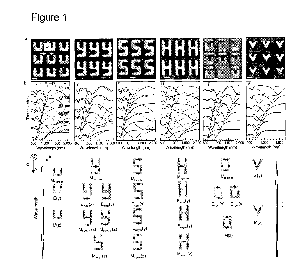
[0073]FIG. 1 shows a series of alphabetical metamaterial structures (FIG. 1a), their optical responses (FIG. 1b), and mode identificafion (FIG. 1c). In order to obtain the tunable optical response from Vis to NIR range, the whole unit cell was minimized along with the dimension of resonators from 100% to 37.5%, which reduces the corresponding bar width (w) from w=80 to 30 nm. FIG. 1b shows the transmission spectra for various alphabetical metamaterials with different widths. The solid curves are spectra taken under Px polarization configurations, while the dashed curves are obtained from Py polarization configurations. Each valley in the transmission spectra represents one resonance mode of metamaterials. The induced electric dipoles due to the alternating field of light lead to two kinds of resonance modes: one is electric mode arising from oscillation of the electric dipoles, while the other is the magnetic mode due to the circular ...
example 3
ion of the SERS Enhancement by Tuning the Laser Wavelength
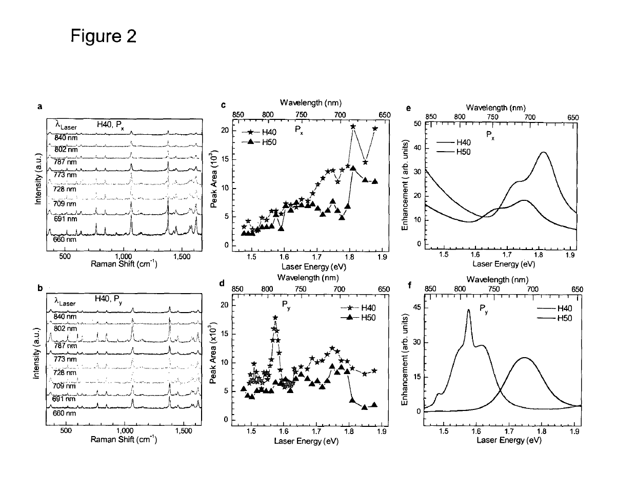
[0076]Alphabetical metamaterials operated in visible-NIR exhibit abundant electric and magnetic dipole modes, and their coupling effect gives further degree of freedom to tune the plasmonic resonance to optimize the SERS effect. The versatile tunability enables the maximization of the strength of local electromagnetic field hot-spots, which dominate the electromagnetic enhancement in SERS effect. It was first shown that the highest SERS signal can be obtained by tuning the laser wavelength using H-shaped metamaterials as an example. FIGS. 2a and 2b display the typical SERS spectra of a monolayer 2-naphthalenethiol bound to H40 sample excited by a tunable laser with Px and Py polarizations, respectively. Considering that laser wavelength (660-840 nm) is far from the first electronic transition (˜242 nm) of 2-naphthalenethiol, it is hypothesized that the enhancement of SERS signal is entirely contributed by the electromagnetic ...
PUM
| Property | Measurement | Unit |
|---|---|---|
| wavelength range | aaaaa | aaaaa |
| width | aaaaa | aaaaa |
| width | aaaaa | aaaaa |
Abstract
Description
Claims
Application Information


