Four-in-one mini-LED module, display screen and manufacturing method

a mini-led module and manufacturing method technology, applied in semiconductor/solid-state device testing/measurement, semiconductor device details, semiconductor devices, etc., to achieve the effect of reducing the number of pin bonding pads, reducing the connection manner of devices, and improving the air tightness and weather resistance of modules

Active Publication Date: 2021-06-01
SHENZHEN ZHIXUNDA OPTOELECTRONICS CO LTD
View PDF15 Cites 0 Cited by
  • Summary
  • Abstract
  • Description
  • Claims
  • Application Information

AI Technical Summary

Benefits of technology

[0036]Advantageous effects of the present invention comprises: the four-in-one mini-LED module, the display screen and the manufacturing method provided by the present invention, on the basis of a packaging module having a plurality of light emitting units originally applied by the applicant, the connection manner of a device is simplified by using the principles of row scanning and field scanning for the operation of the display screen, so that the number of pin bonding-pads is reduced by half; by using the principle of BGA packaging, the air tightness and weather resistance of the module are ensured, the service life of the device is prolonged, and the module can achieve packaging of a smaller size; an electrical connection is achieved by placing R chips of the same column on the same electrical connection region due to the fact that the chip-substract of the R chip is an electric conductor, thus simplifying the connection line, reducing the number of conductive holes, and shortening the pitch accordingly; by providing an optical virtual isolation region, the problem of light mixing of the packaging module is solved, and the sharpness and definition of the display screen are improved; by separately leading out the first electrode of the R chip and separately supplying power, the problem of power waste is solved; and by providing the bonding-pads inside the bottom of the substrate and providing a multilayer substrate, the problem of air tightness of the packaging module is effectively solved, the weather resistance of the device is improved, and the service life of the device is prolonged.
of the present invention comprises: the four-in-one mini-LED module, the display screen and the manufacturing method provided by the present invention, on the basis of a packaging module having a plurality of light emitting units originally applied by the applicant, the connection manner of a device is simplified by using the principles of row scanning and field scanning for the operation of the display screen, so that the number of pin bonding-pads is reduced by half; by using the principle of BGA packaging, the air tightness and weather resistance of the module are ensured, the service life of the device is prolonged, and the module can achieve packaging of a smaller size; an electrical connection is achieved by placing R chips of the same column on the same electrical connection region due to the fact that the chip-substract of the R chip is an electric conductor, thus simplifying the connection line, reducing the number of conductive holes, and shortening the pitch accordingly; by providing an optical virtual isolation region, the problem of light mixing of the packaging module is solved, and the sharpness and definition of the display screen are improved; by separately leading out the first electrode of the R chip and separately supplying power, the problem of power waste is solved; and by providing the bonding-pads inside the bottom of the substrate and providing a multilayer substrate, the problem of air tightness of the packaging module is effectively solved, the weather resistance of the device is improved, and the service life of the device is prolonged.

Problems solved by technology

Thus, the light emitting diodes (LEDs) were developed, but the application of the LEDs had not gained much attention later.
But its brightness limits the use under natural light, so an LED display (screen) is developed, which has the characteristics of large viewing angle, high brightness, and colorfulness.
However, as the pixel pitch of the LED display screen is reduced, the number of packaging devices per unit area is increasing, which makes the packaging difficulty increase exponentially.
As the number of packaging devices per unit area increases, the mounting workload and the mounting difficulty will be also greatly increased.
However, COB packaging has not been widely used in the field of LED display screens so far.
The reason is that the panel ink color of COB packaging is not well controlled.
When a lamp is not turned on, the surface ink color is inconsistent.
The center value difference or the ink difference of substrates of different batches of chips lead to color difference, and the entire screen consistency is poor.
Besides, the chip is directly mounted on a circuit board and lacks of protection, so that the reliability cannot be guaranteed, and the maintenance cost of an ineffective LED chip is high.
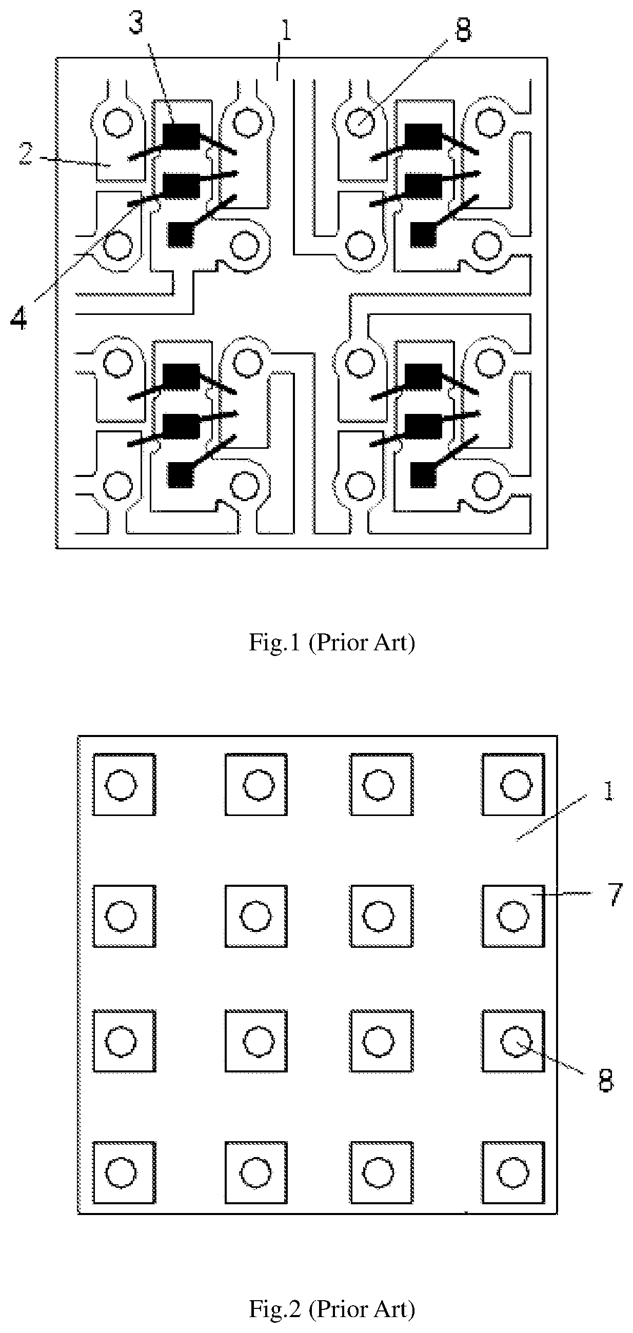
First, there are too many pin bonding-pads on the back surface of the substrate. The existing small-pitch display screens mainly use 1515, 1010, 0808, 0606, 0505 and other types of packaging devices, all of which are 4-pin devices, one anodes or cathodes of red chips, green chips and blue chips are connected in parallel through a common-anode or a common-cathode manner, and the other pin is separately led out. When the solutions of the patents such as CN106847801A and CN106847800A are used, a plurality of light-emitting units are integrated into one packaging module, but the number of pins is not reduced. As shown in FIG. 2, firstly, the more light-emitting units is integrated, the more pins there is. As a result, the leading-wiring of the PCB becomes more complicated in the subsequent production process, and the design of a test socket is relatively more difficult when the test process is performed.
Secondly, with the further reduction of the size of the LED module, the number of bonding-pads on the bottom of the substrate is too large, besides, some bonding-pads are even on the bottom edge of the substrate, which causes the problem of soldering tin leakage at the time of soldering, thereby affecting the visual effect of a finished product. The spilled tin in contact with the surrounding bonding-pads also easily leads to short-circuit devices.
Second, there are the problems of excessive plated-through holes and a complicated electrode connection line on the front surface of the substrate. In the production of packaging modules, the substrate is etched according to the designed line to facilitate subsequent electroless copper deposition and copper electroplating, die bonding and wire bonding, as shown in FIG. 4, but the above patents have complicated circuit design and excessive plated-through holes. Each connection region on the front surface of the substrate needs to be set plated-through holes. If it is necessary to reduce the number of bottom bonding-pads, the connection line is more complicated, and the number of via holes is even more, which makes it difficult to further reduce the size of the packaging module.
Third, there is a problem of short service life. In the production of RGB-LED packaging modules, an etching line is usually designed on the substrate, then electroless copper deposition and copper electroplating is performed, an RGB-LED chip is then arranged, die bonded and wire bonded, a layer of epoxy resin glue is molded on the chip, and finally, the substrate is cut to obtain a target module. However, the edge of the module obtained after cutting will have a cut metal line, as shown in FIG. 1, which is usually gold-plated copper. As time goes by, because a metal material and a resin material are different materials, the bonding performance is poor, and the joint of gold-plated copper and epoxy resin glue at the edge will be delaminated, which directly affects the air tightness of the packaging module, resulting in reduction of life of the packaging module. In actual production, some people solve the problem of delamination by using a manner of spraying a surface treating agent on the surface of the metal material, but the cost will be correspondingly improved.
Fourth, there is a problem of low soldering yield. The bonding-pads of the existing LED module are lower or uneven in height, and this is especially obvious in the case of a large number of pin bonding-pads. In the subsequent product process, the LED module is usually soldered to the PCB, but due to the fact that the bonding—are lower or uneven in height, it may lead to the problems that short circuit occurs or some bonding-pads are not successfully soldered during soldering
Fifth, the produced LED display screen has low sharpness and is prone to the problem of light mixing. In the LED display screen, RGB LEDs are mixed in a same optical medium to form a mixed color light emission. In the single-package, after single LEDs are spliced and combined, light sources are independent, and there is a gap between one light source and another light source, which is not easy to cause a phenomenon of light mixing, and the sharpness thereof is relatively high. In the packaging module, there are a plurality of light-emitting units on the substrate, the plurality of light-emitting units are molded with the same glue layer. As shown in FIG. 3, different light-emitting units are in the same light guide medium. When light is reflected, diffused and scattered in the same optical medium, a plurality of light-emitting units may be prone to light mixing and color mixing, thus affecting the sharpness and definition of the LED display screen.
Sixth, there is a problem of power waste.
Although this solution is simple and easy, it has two major drawbacks: first, the divider resistor generates a large amount of useless power, which greatly increases the overall power consumption of application terminal products; second, heat generated by the divider resistor increases the heat dissipation burden of the application terminal products, and affects the reliability and service life of the products.
Seventh, there is a problem of device heat dissipation.
The problem of heat dissipation has always been a problem that restricts the development of the LED industry.
If the temperature is too high, the LED will lose efficacy directly.
In the LED display screen, there are millions of LEDs working at the same time, which will generate a lot of heat.
The above patent fails to effectively solve this problem.
Therefore, the prior art has yet to be improved and developed.

Method used


Image

  • Four-in-one mini-LED module, display screen and manufacturing method
  • Four-in-one mini-LED module, display screen and manufacturing method
  • Four-in-one mini-LED module, display screen and manufacturing method

Examples


Embodiment Construction

[0051]Implementations of the present invention are described in detail below, and the examples of the implementations are illustrated in the drawings, where the same or similar reference numerals throughout indicate the same or similar elements or elements having the same or similar functions. The implementations described below with reference to the drawings are exemplary, only intended to be illustrative of the present invention and not to be construed as limiting to the present invention.

[0052]In the description of the present invention, it should be understood that orientation or position relationships indicated by the terms such as “center”, “longitudinal”, “transverse”, “length”, “width”, “thickness”, “up”, “down”, “front”, “rear”, “left”, “right”, “vertical”, “horizontal”, “top”, “bottom”, “inside”, and “outside” are based on orientation or position relationships shown in the accompanying drawings, and are used only for ease and brevity of illustration and description of the ...


PUM

PropertyMeasurementUnit
infrared emissivityaaaaaaaaaa
driving voltageaaaaaaaaaa

Abstract

Disclosed is a four-in-one mini-LED module, a display screen, and a manufacturing method thereof. The four-in-one mini-LED module comprises a substrate and a plurality of RGB-LED chip sets arranged in an array on the substrate. The RGB-LED chip sets are provided with glue layers. Each RGB-LED chip set comprises an R chip, a G chip and a B chip, each chip has a first electrode and a second electrode, and the first electrode and the second electrode have opposite polarities. The first electrodes of all the chips of the same row are electrically connected, the second electrodes of all the R chips of the same column are electrically connected, the second electrodes of all the G chips of the same column are electrically connected, and the second electrodes of all the B chips of the same column are electrically connected.

Description

CROSS REFERENCE TO RELATED APPLICATIONS[0001]The present application claims the benefit of Chinese Patent Application No. 201810610475.0 filed on Jun. 14, 2018, the contents of which are incorporated herein by reference in its entirety.TECHNICAL FIELD[0002]The present invention relates to an LED packaging technology, and more particularly relates to a four-in-one mini-LED module, a display screen, and a manufacturing method.BACKGROUND ART[0003]LEDs were born in 1923. When Rousseff studied a semiconductor sic, he discovered that an impurity-doped p-n junction emits light after being energized. Thus, the light emitting diodes (LEDs) were developed, but the application of the LEDs had not gained much attention later. With the rapid development of the electronic industry, in the 1960s, the display technology had developed rapidly, and various display technologies are developed such as plasma display panels, LED liquid crystal displays, and light emitting diodes (LED). As semiconductor m...

Claims


Application Information

Patent Timeline
Patent Type & Authority Patents(United States)
IPC IPC(8): H01L25/075H01L21/66H01L23/00H01L33/56H01L33/62H01L33/64
CPCH01L25/0753H01L22/12H01L24/48H01L33/56H01L33/62H01L33/647H01L2224/48227H01L2924/12041H01L2933/005H01L2933/0066H01L2933/0075H01L2224/97
Inventor KONG, YIPINGYUAN, XINCHENGZHOU, MINKANG
Owner SHENZHEN ZHIXUNDA OPTOELECTRONICS CO LTD
Why Eureka
Try Eureka