
Systems and methods for controlling the morphology and porosity of printed reactive inks for high precision printing

a reactive ink and printing technology, applied in the field of systems and methods for controlling the morphology and porosity of printed reactive inks for high precision printing, can solve the problems of complex patterning process, multiple steps of electroless plated contacts, and the inability to achieve high quality of existing techniques, so as to achieve high performance, reduce capital expenditures, and increase the maximum sustainable growth rate and profit margin.

Active Publication Date: 2021-08-03
ARIZONA STATE UNIVERSITY
View PDF48 Cites 0 Cited by
  • Summary
  • Abstract
  • Description
  • Claims
  • Application Information

AI Technical Summary

Benefits of technology

[0005]The present invention relates to systems and methods for the morphological control of reactive inks for high precision printing and a particular implementation in photovoltaic manufacturing techniques. More particularly, DoD printing can act as a disruptive technology for solar cell technologies. DoD printing offers a low-cost, high performance alternative to traditional methods used in the manufacturing and processing of silicon solar cell technologies. A single DoD printer can carry out numerous tasks replacing the need to purchase equipment, resulting in significant reductions in capital expenditures with higher maximum sustainable growth rates and profit margins. DoD printing offers precise placement of materials with minimum waste, and good alignment without contact. This invention disclosure details a controllable approach for patterning dopants / seed layers and etching grooves at different scales in a cost efficient manner.
[0008]In various embodiments, the invention provides methods and systems that utilize dispensing printing for patterning of surfaces and materials, applicable to solar cell technologies. Patterning of surfaces can be performed using various different techniques depending on the end goal for which the patterning is done including, for example, the removal or deposition of materials designed / selected specifically for electronics, clinical, or biological applications. Some specific techniques for selective patterning of solar cell technologies may include, for example, photolithography, soft lithography, laser processing, screen printing, aerosol printing, and inkjet printing. Each of these existing techniques has limitations in achieving high quality results while also having low capital expenditure and waste, industrial scalability, and process simplicity. The challenge of patterning surfaces of solar cell technologies can be exemplified by plated contacts. Some manufacturing techniques for electro-plated contacts, electroless-plated contacts, and light-induced-plated contacts require multi-step, complex and costly patterning processes that often require micron-scale alignment from one step to the next. Solar cell technologies beyond plated contacts can also be improved by more cost efficient, simplified processes through high precision patterning, resulting in reduced capital expenditure.
[0009]In some embodiments, the invention provides methods and systems for selective patterning techniques that use high precision dispensing printing to: (i) directly remove a patterned region of a material; (ii) selectively pattern a region to be doped directly below where the contacts will be formed, (iii) directly selectively pattern a seed layer for subsequent deposition of contacts (i.e., plated contact), and / or (iv) isolate edges to prevent shunting.
[0012]In yet another embodiment, the invention provides a method for selectively patterning a solar cell device using high precision dispensing printing to directly selectively pattern a seed layer for subsequent deposition of contacts (i.e., plated contacts). The patterning of the seed layer can include, in some embodiments, direct removal of a patterned region from a material and / or selectively patterning of a regions to be doped directly below where the contacts will be formed, coupled with subsequent printing of well-controlled, precise features to form a seed layer or metallization layer. The printed seed or metallization layer may be formed, for example, from reactive inks or particle-based inks. The chemistry of the inks may be adjusted to modify the surface tension and wetting of the droplets, and masks may be used to control the flow of the inks.
[0013]In another embodiment, the invention provides a method for selectively dispensing the reactive inks onto the polymeric encapsulants commonly used for solar cell encapsulation (PET, TPO, EVA, Ionomers, etc) without the need for printing on the cells. Electrical contact is ensured by contacting the polymer and the cells through the process of encapsulation. The chemistry of the inks may be adjusted to modify the surface tension and wetting of the droplets, and masks may be used to control the flow of the inks on the polymeric substrates.
[0014]In still another embodiment, the invention provides a method for selectively patterning a solar cell device using high precision printing to isolate edges to prevent shunting. In some embodiments, precise edge isolation to isolate shunts is performed subsequent to directly removing a patterned region of a material, selectively patterning a region to be doped directly below where contacts will be formed, and / or directly selectively patterning a seed layer for subsequent deposition of contacts. The edge isolation can be achieved through etching a groove near an edge of a wafer where, in some embodiments, the groove can act as the edge isolation and, in other embodiments, the groove can acts as a cleave line to completely remove the edges from the wafer. The chemistry of the etchant may be adjusted to modify the surface tension and wetting of the droplets, and masks may be used to control the flow of the etchants.

Problems solved by technology

More particularly, DoD printing can act as a disruptive technology for solar cell technologies.
Each of these existing techniques has limitations in achieving high quality results while also having low capital expenditure and waste, industrial scalability, and process simplicity.
Some manufacturing techniques for electro-plated contacts, electroless-plated contacts, and light-induced-plated contacts require multi-step, complex and costly patterning processes that often require micron-scale alignment from one step to the next.

Method used

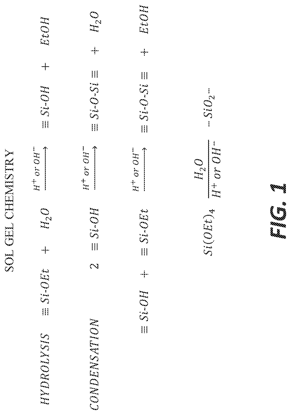

Image

  • Systems and methods for controlling the morphology and porosity of printed reactive inks for high precision printing
  • Systems and methods for controlling the morphology and porosity of printed reactive inks for high precision printing
  • Systems and methods for controlling the morphology and porosity of printed reactive inks for high precision printing

Examples


example 1

[0084]As described above, the dispensing RSI printing process of FIGS. 8A, 8B, and 8C is performed using the printing system of FIG. 7. The base ink for RSI was prepared with 1.0 g silver acetate (C2H3AgO2, anhydrous 99%, Alfa Aesar) dissolved in 2.5 mL ammonium hydroxide (NH4OH, 28-30 wt %, ACS grade, BDH Chemicals). The solution was then stirred for 2 minutes on a vortex mixer to dissolve the silver acetate. Next, 0.2 mL of formic acid (CH2O2, >=96%, ACS reagent grade, Sigma Aldrich) was added in two steps with a quick stir at the end of each step. The ink was then allowed to sit for 12 hours before being filtered through a 450 nm nylon filter.

[0085]This base ink was then diluted 1:1 or 10:1 by volume with ethanol (EtOH, C2H6O, ACS reagent grade, Sigma Aldrich) to increase the stability of the droplets for printing contact pads (7×7 mm2) on glass slides for bulk resistivity measurements. The diluted ink was then filtered again through the 450 nm nylon filter immediately before use...

example 2

[0096]The base ink for RSI was prepared with 1.0 g of silver acetate (C2H3AgO2, anhydrous 99%, Alfa Aesar) was dissolved in 2.5 mL ammonium hydroxide (NH4OH, 28-30 wt %, ACS grade, BDH Chemicals). The solution was then stirred for 2 minutes on a vortex mixer to dissolve the silver acetate. Next, 0.2 mL of formic acid (CH2O2, ≥96%, ACS reagent grade, Sigma Aldrich) was added in two steps with a quick stir at the end of each step. The ink was then allowed to sit for 12 hours before being filtered through a 450 nm nylon filter. For this example, the RSI was diluted 1:1 by volume with ethanol (EtOH, C2H6O, ACS reagent grade, Sigma Aldrich) and then filtered again through the 450 nm nylon filter immediately before use.

[0097]RSI metallization features were printed in ambient atmosphere on a Microfab Jetlab II inkjet printing system. The Jetlab II is equipped with an MJATP-01 piezoelectric-driven print head with 60-μm-wide nozzle. Samples were printed with the substrate held between 51° C....

example 3

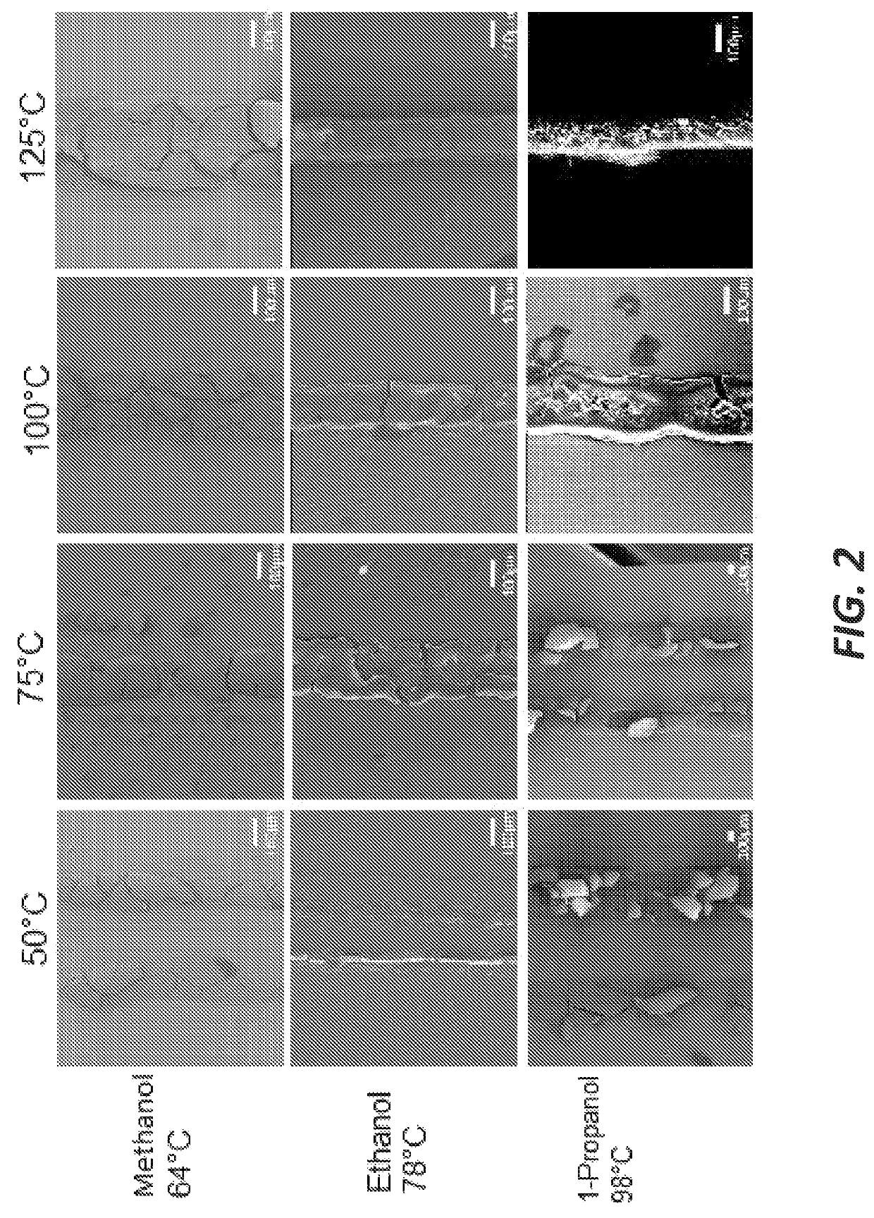
[0114]Most prior studies on low-temperature reactive inks are investigations with the ink printed at room temperature, allowed to dry, and then sintered at elevated temperatures to improve the material properties. These studies have not explored the unique role that temperature and solvent evaporation play in controlling the in situ reduction rates and morphology of the printed structures. While most work provides top-down images of their printed silver, detailed information regarding the porosity and cross-section morphology is lacking. In this example, it is demonstrated how the porosity of silver structures printed with diaminesilver (I) inks can be controlled from 93% porosity down to 50% porosity by adjusting solvent vapor pressure, solvent viscosity, and substrate temperature. These results take advantage of the increase in reduction reaction rate and solvent evaporate rate that occurs at elevated temperatures when solvents with low surface energy and high vapor pressures are ...


PUM

PropertyMeasurementUnit
temperatureaaaaaaaaaa
porosityaaaaaaaaaa

Abstract

Systems and methods for optimizing morphology and electrical properties of silver printed on a substrate with a particular implementation in photovoltaic manufacturing techniques. The system comprises a substrate, a printer jet head having a nozzle to dispense a reactive metal ink and a solvent onto the substrate, and wherein the solvent and a temperature of the substrate are controlled during deposition of the reactive metal ink onto the substrate to produce a dense film in the absence of sintering.

Description

CROSS-REFERENCE TO RELATED APPLICATION(S)[0001]This application is a PCT international application and claims the benefit of U.S. Provisional Patent Application No. 62 / 507,686, filed on May 17, 2017, the entire contents of which are incorporated herein by reference.BACKGROUND OF THE INVENTION[0002]The processes currently used to manufacture photovoltaic devices are suitable to achieve a minimum sustainable price, but low profit margins and high capital expenditures on numerous pieces of equipment severely limit the growth capacity, while also preventing introduction of newer innovative technologies into the market.[0003]Approximately 2 Mkg of silver ink and pastes are consumed each year. While the vast majority of this silver is consumed as silver paste to metalize photovoltaic panels, there is substantial interest in drop-on demand (DoD) printable silver inks for low-cost electronics fabrication and rapid prototyping of electronic circuits. Most commercially available DoD silver in...

Claims


Application Information

Patent Timeline
Patent Type & Authority Patents(United States)
IPC IPC(8): B41J2/16C08K3/08C09D11/36C09D11/38C09D11/52
CPCB41J2/1607C08K3/08C09D11/36C09D11/38C09D11/52
Inventor BERTONI, MARIANAJEFFRIES, APRILHILDRETH, OWENMAMIDANNA, AVINASH
Owner ARIZONA STATE UNIVERSITY
Learn More