Gallium nitride single crystal substrate and method of proucing same

a technology of gallium nitride and single crystal substrate, which is applied in the direction of polycrystalline material growth, crystal growth process, chemically reactive gas, etc., can solve the problems of lack of cleavage plane, electrical insulation, and inability to produce large gan substrates at presen

Inactive Publication Date: 2002-01-31
SUMITOMO ELECTRIC IND LTD
View PDF0 Cites 104 Cited by
  • Summary
  • Abstract
  • Description
  • Claims
  • Application Information

AI Technical Summary

Problems solved by technology

But a large GaN substrate cannot be produced at present yet.
The impossibility of making a GaN substrate forces the manufacturers to adopt a sapphire substrate for making blue GaInN LEDs.
One of the drawbacks is the lack of cleavage planes.
A further weak point is electrical insulation.
Non-cleavage, rigidity and insulation are drawbacks of sapphire as a substrate material.
It is difficult to cut the sapphire wafer due to the rigidity and the non-cleavage.
The mechanical polished surface is inferior to the natural cleavage planes in the reflection property.
This is an extra drawback of making a laser diode of GaInN.
The non-cleavage raises the difficulty of dicing the sapphire wafer into chips.
The difficulty of dicing raises the cost of producing GaInN LEDs.
The greatest drawback of the sapphire substrate is the lack of cleavage in any cases.
SiC is, however, a highly expensive material.
There is no matured technology of producing SiC bulk single crystals on a large scale yet.
The difficulty of supply would raise the cost of GaInN LEDs, if GaInN films were to be piled upon an SiC substrate.
The present technology cannot produce SiC-based GaInN LEDs on a large scale at a lower cost than sapphire-based GaInN LEDs.
There is poor probability for SiC substrates in overcoming sapphire substrates.
SiC is not a promising material as a substrate of GaN-like semiconductors.
The sapphire substrate induces a problem of a big defect density in the epitaxial GaN-like films due to the difference of the lattice constant between GaN and sapphire (Al.sub.2 O.sub.3).
In the case of a GaInN laser, it is supposed that the high density of defects in GaN or GaInN films may res

Method used


Image

  • Gallium nitride single crystal substrate and method of proucing same
  • Gallium nitride single crystal substrate and method of proucing same
  • Gallium nitride single crystal substrate and method of proucing same

Examples


embodiment 1

[0069] [ GaN / GaAs: HVPE method: three kinds of HCl gases]

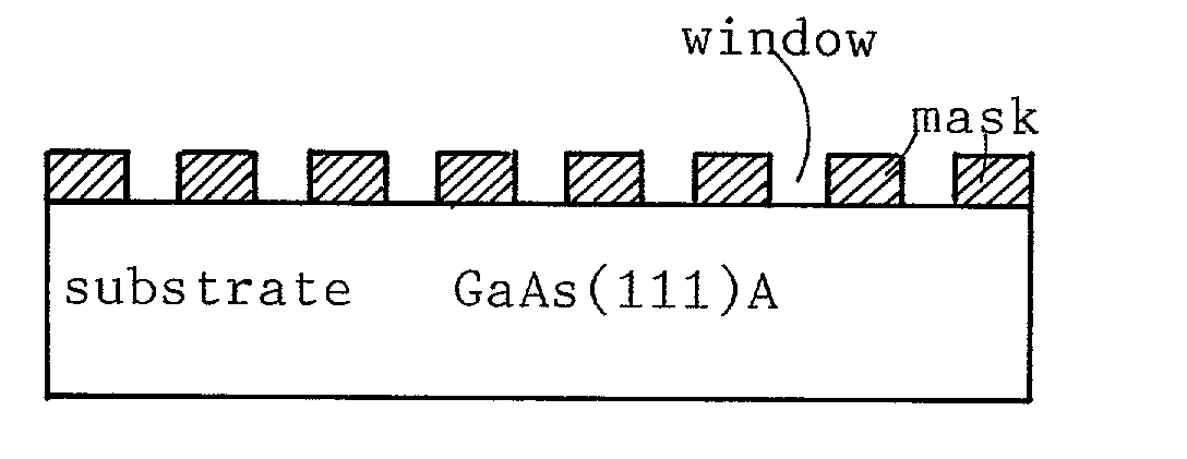
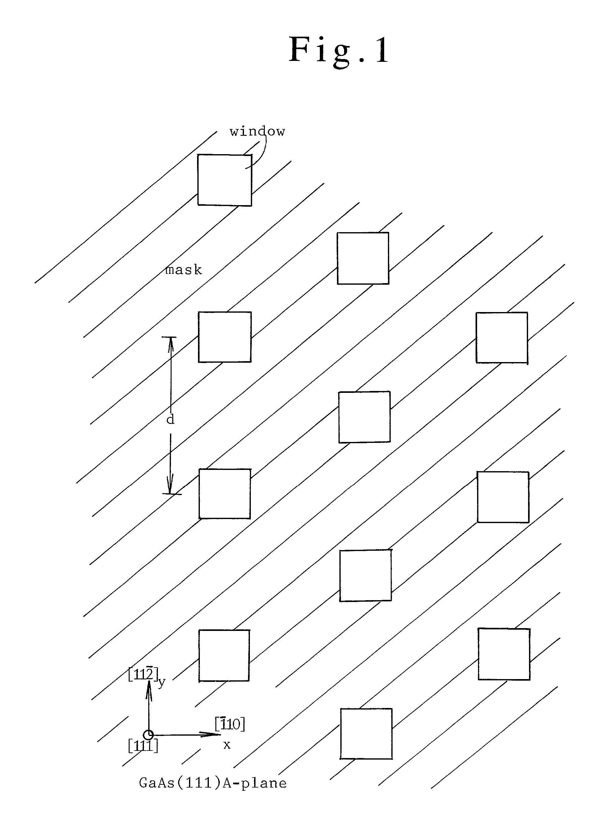
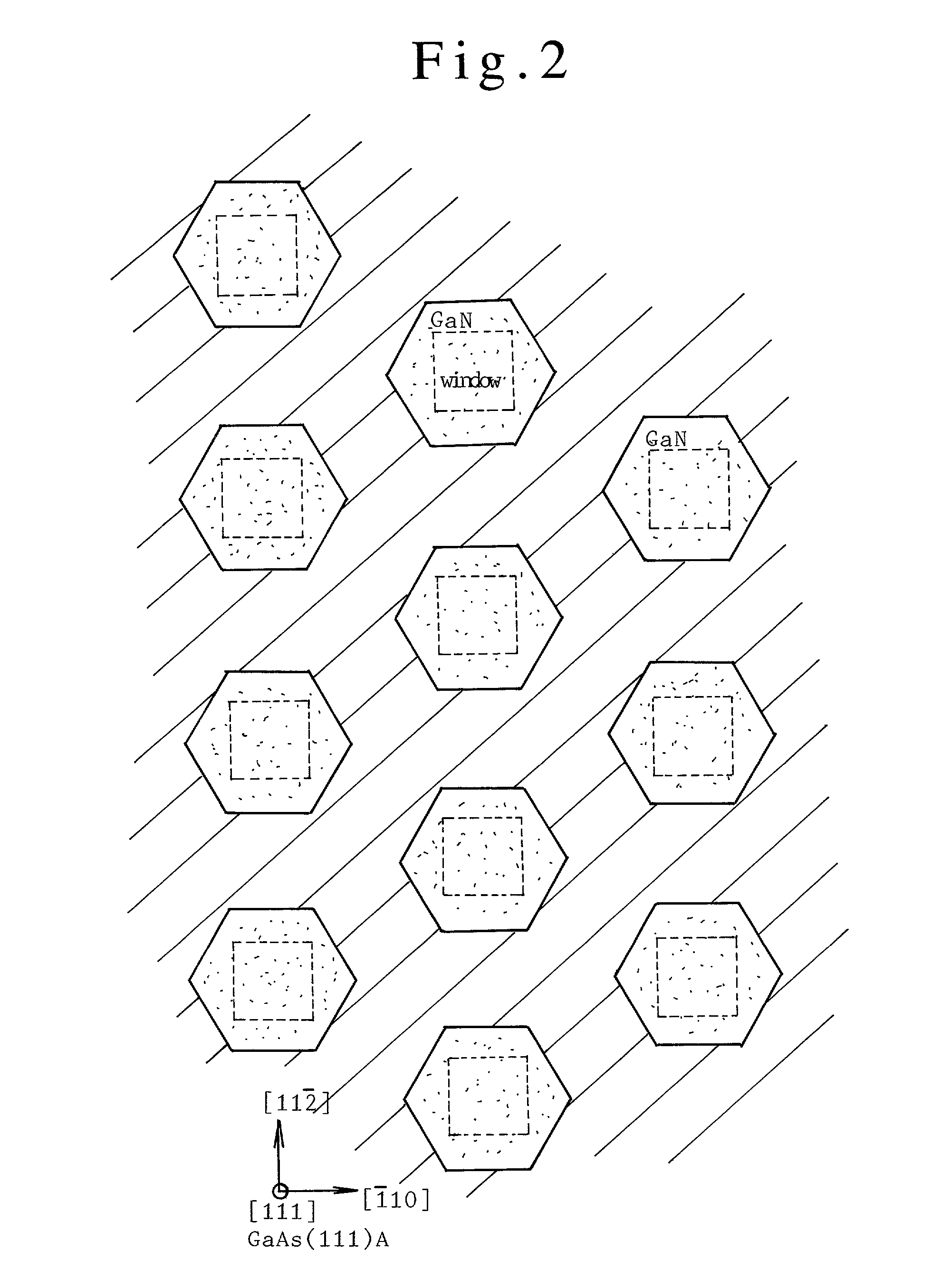
[0070] A GaAs(111) wafer is prepared for a substrate crystal. A silicon dioxide (SiO.sub.2) insulating film is formed uniformly upon the GaAs(111)A plane. Photolithography perforates a plenty of dottedly-populated square windows on the SiO.sub.2 mask for revealing the undercoat GaAs surface partially within the windows, as shown in FIG. 1. Each window is a square of a 2 .mu.m long side. A set of dotted windows align with a 4 .mu.m long spatial period (d=4 .mu.m) in series in parallel with -direction of the GaAs substrate. Being distanced by 3.5 .mu.m(=3.sup.1 / 2 d / 2) in vertical direction , a second set of windows align with a half period shift with the same period in series in the same direction as the former set. A third set of windows align with a half period shift with the same period in the same direction as the former sets. Similar alignments of windows are repeated on the mask. The centers of the nearest neighboring thre...

embodiment 2

[0087] [ GaN / GaAs; HVPE method; H.sub.2O added HCl gas]

[0088] A GaN crystal is made on a GaAs substrate by a similar manner to embodiment 1. Namely, a GaN buffer layer and a GaN epitaxial layer are produced upon a masked GaAs wafer by a HVPE method supplying HCl+H.sub.2 to a Ga melt for converting Ga to GaCl and supplying NH.sub.3+H.sub.2 for making NH.sub.3 react with GaCl, and making GaN on the GaAs substrate. Embodiment 2 differs from embodiment 1 at the HCl+H.sub.2 gas which is supplied to the Ga-melt. Instead of HCl including water, hydrogen H.sub.2 gas contains water. The prepared gases are;

[0089] (d) high purity HCl gas refined several times,

[0090] (e) humid hydrogen gas produced by bubbling ultrapure water with hydrogen gas.

[0091] A mixture of (d) and (e) at an arbitrary rate is supplied to the heated Ga-melt in the HVPE furnace. The rate H.sub.2O / HCl is continually varied in a range between 0 and 3000 ppm. Namely, 0.ltoreq.H.sub.2O / HCl.l-toreq.3000 ppm. In the first reactio...

embodiment 3

[0092] [EMBODIMENT 3; GaN / GaAs: HVPE method; O.sub.2 added HCl gas]

[0093] Embodiment 3 makes a GaN single crystal film upon a masked GaAs substrate wafer in a similar way to embodiment 1. Like embodiment 1, a GaN buffer layer and a GaN epitaxial layer are grown by the HVPE method on a GaAs substrate by utilizing a mask having windows positioned at corners of equilateral triangles. The HCl gas is different from that of embodiment 1. Instead of water, oxygen is intentionally added to the HCl gas. Embodiment 3 introduces oxygen into the GaCl gas through the HCl gas. Prepared gases are;

[0094] (f) high purity HCl gas refined several times,

[0095] (g) high purity oxygen gas.

[0096] A mixture (HCl+O.sub.2) of (f) and (g) at an arbitrary rate is supplied to the heated Ga-melt in the HVPE furnace. The rate O.sub.2 / HCl is continually varied in a range between 0 and 3000 ppm. Namely, 0.ltoreq.O.sub.2 / HCl.ltoreq.3000 ppm. In the first reaction of 2Ga+2HCl.fwdarw.2GaCl+H.sub.2, oxygen included in ...


PUM


Abstract

An n-type GaN substrate having a safe n-type dopant instead of Si which is introduced by perilous silane gas. The safe n-dopant is oxygen. An oxygen doped n-type GaN free-standing crystal is made by forming a mask on a GaAs substrate, making apertures on the mask for revealing the undercoat GaAs, growing GaN films through the apertures of the mask epitaxially on the GaAs substrate from a material gas including oxygen, further growing the GaN film also upon the mask for covering the mask, eliminating the GaAs substrate and the mask, and isolating a freestanding GaN single crystal. The GaN is an n-type crystal having carriers in proportion to the oxygen concentration.

Description

[0001] 1. Field of the Invention[0002] This invention relates to a gallium nitride (GaN) single crystal substrate and a method of making same for producing a light emitting diode (LED) and a laser diode (LD) or a field effect transistor (FET) making use of the group III-V nitride compound semiconductors, in particular, to an n-type GaN substrate and a method of making the n-type GaN substrate. In this description, the impurity which determines the conduction type of a semiconductor is called a dopant for discerning the conduction-type determined impurity from the other impurities.[0003] Among the periodic-table group III-V compound semiconductors, large substrate crystals can be produced only for gallium arsenide (GaAs), indium phosphide (InP) and Gallium phosphide (GaP). These semiconductors allow us to produce large-scaled bulk crystals by the Bridgman method or the Czochralski method. Substrate wafers are prepared by slicing the large and long single crystal ingots of GaAs, InP o...

Claims


Application Information

Patent Timeline
IPC IPC(8): H01L21/20H01L21/205H01L33/00
CPCC30B25/02C30B29/406H01L21/02395H01L21/02433H01L21/02458H01L21/0254H01L33/0079H01L21/0262H01L21/02639H01L21/02647H01L21/02664H01L33/0075H01L21/02576H01L33/0093
Inventor MOTOKI, KENSAKUOKAHISA, TAKUJIMATSUMOTO, NAOKIMATSUSHIMA, MASATO
Owner SUMITOMO ELECTRIC IND LTD
Why Eureka
Try Eureka