Method and apparatus for simulating physical fields

a physical field and method technology, applied in image data processing, analogue and hybrid computing, complex mathematical operations, etc., can solve the problems of many spurious additional nodes, slow down or even fail the optimization process, and increase the complexity of the optimization process, so as to achieve the effect of improving the structur

Inactive Publication Date: 2002-04-11
INTERUNIVERSITAIR MICRO ELECTRONICS CENT (IMEC VZW)
View PDF0 Cites 35 Cited by
  • Summary
  • Abstract
  • Description
  • Claims
  • Application Information

AI Technical Summary

Benefits of technology

0086] where said n-dimensional mesh is used to create an improved structure.

Problems solved by technology

Concerning the mesh, one of the issues is to perform the optimization using the appropriate amount of nodes at the appropriate location.
On the other hand, if the total amount of nodes increases, the complexity increases and the optimization process slows down or even can fail.
The disadvantage is that during mesh refinement many spurious additional nodes are generated in regions where no mesh refinement is needed.
Therefore mesh refinement still generates a number of spurious points.
The disadvantage is that programming requires a lot of work in order to allow for submission of arbitrary complicated domains.
Furthermore, adaptive meshing is possible but obtuse triangles are easily generated and one must include algorithms to repair these deficiencies, since numerical stability and numerical correctness suffers from obtuse triangles.
As a consequence, mesh refinement and in particular adaptive meshing, generates in general spurious nodes.
For instance, the on-chip interconnect structure in modern ULSI integrated circuits is a highly complex electromagnetic system.
As a consequence, analytic solution methods have only limited applicability and numerical or computer-aided design methods need to be used.
The continuous down-scaling of the pitch implies that parasitic effects become a major design concern.
Furthermore, interconnect delay will soon become the main bottleneck for increasing the operation frequencies of the fully integrated circuit.
However, this is only a current limit.
These methods introduce three types of errors.
Firstly, there is the error caused by solving for a discrete mesh, which is only an approximation to a continuum.
Secondly, the finite difference methods require an iterative solution, which is terminated after a certain time--this implies a residual error.
However, varying mesh sizes places limitations on the continuity of the solution resulting in unnecessary nodes being created to provide sufficiently gradual changes.
Hence, conventionally a large amount of storage space and high-powered computers are required to achieve an accurate result in a reasonable amount of time.

Method used


Image

  • Method and apparatus for simulating physical fields
  • Method and apparatus for simulating physical fields
  • Method and apparatus for simulating physical fields

Examples


examples

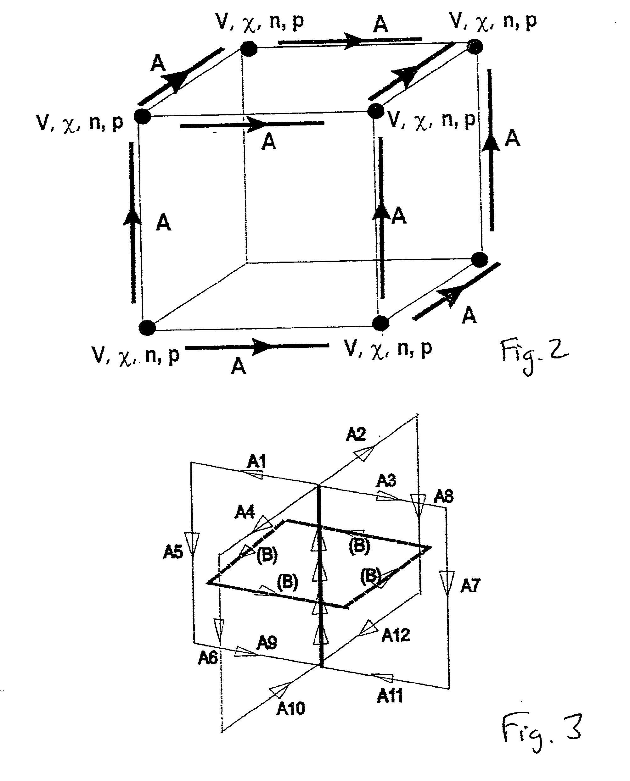
[0314] A number of examples are presented demonstrating that the proposed potential formulation in terms of the Poisson field V, the vector field A and the dummy field .chi., is a viable method to solve the Maxwell field problem. All subtleties related to that formulation, i.e. the positioning of the vector potential on links, and the introduction of the ghost field .chi., have already been described above in constructing the solutions of the static equations. Therefore, a series of examples in the static limit are presented.

[0315] Metal Plug on Highly-doped Silicon

[0316] The first example concerns the electromagnetic behavior of a metal plug on (highly-doped) silicon. This example addresses all subtleties that are related to metal-semiconductor, metal-insulator and semiconductor-insulator interfaces as well as triple lines. The simulation region (10.times.10.times.10 .mu.m.sup.3) consists of two layers. A layer of the silicon (5 .mu.m) is highly doped at the top, using a square mas...


PUM


Abstract

In order to design on-chip interconnect structures in a flexible way, a CAD approach is advocated in three dimensions, describing high frequency effects such as current redistribution due to the skin-effect or eddy currents and the occurrence of slow-wave modes. The electromagnetic environment is described by a scalar electric potential and a magnetic vector potential. These potentials are not uniquely defined, and in order to obtain a consistent discretization scheme, a gauge-transformation field is introduced. The displacement current is taken into account to describe current redistribution and a small-signal analysis solution scheme is proposed based upon existing techniques for static fields in semiconductors. In addition methods and apparatus for refining the mesh used for numerical analysis is described.

Description

[0001] The present application claims priority to and incorporates by reference, in their entirety, U.S. application Ser. No. 60 / 213,7964, titled "METHOD AND APPARAUTS FOR SIMULATING ELECTROMAGENTIC FIELDS" filed Jun. 23, 2001 and European Application No. 0113039.2, titled "AB INITIO ELECTRODYNAMIC MODELING OF ON-CHIP BACK-END STRUCTURES", filed May 30, 2001.[0002] The present invention relates to a method and apparatus for simulating fields especially electromagnetic fields, particularly useful in the context of analysis of interconnect structures, is presented.[0003] Many problems in engineering, physics and chemistry require solving systems of partial differential equations of the type: 1 J ( k ) + ( k ) t= S ( k );[0004] k being a positive whole number[0005] In this equation (equation 1), J represents a flux of a substance under consideration whose density is given by .rho. and S represents some external source / sink of the substance. To mention a few examples:[0006] Electrical e...

Claims


Application Information

Patent Timeline
Patent Type & Authority Applications(United States)
IPC IPC(8): G06F17/13G06F17/17G06F17/50G06T17/20
CPCG06F17/13G06F17/175G06F17/5018G06T17/205G06F2217/16G06T17/20G06F17/5036G06F30/23G06F30/367G06F2111/10
Inventor MEURIS, PETERSCHOENMAKER, WIMMAGNUS, WIM
Owner INTERUNIVERSITAIR MICRO ELECTRONICS CENT (IMEC VZW)
Why Eureka
Try Eureka