Semiconductor device

a technology of semiconductor devices and dielectric devices, applied in semiconductor devices, semiconductor/solid-state device details, electrical apparatus, etc., can solve the problems of less reliable devices, dispersed resistance, and inability to connect materials, so as to minimize the increase and prevent dishing and erosion, and effectively minimize the effect of dispersion of interconnect resistan

Inactive Publication Date: 2003-06-05
NEC ELECTRONICS CORP
View PDF23 Cites 9 Cited by
  • Summary
  • Abstract
  • Description
  • Claims
  • Application Information

AI Technical Summary

Benefits of technology

0054] In this invention, when there is an interconnect area where a plurality of copper interconnects extend over 100 .mu.m or more in one direction (area (a)), it is desirable to set unique design criteria for the area. Specifically, a line/space ratio in copper interconnects in area (a) is preferably 4.5 or less, more preferably 4 or less, most preferably 3 or less. It may, as described later in Example 2, effectively prevent dishing and erosion and minimize increase and dispersion in an interconnect resistance. There are no restrictions for a lower limit for the line/space ratio, but it is preferably 0.5 or higher...

Problems solved by technology

Copper as an interconnect material cannot be, however, anisotropically etched by RIE (Reactive Ion Etching), and thus is generally subject to a damascene process employing CMP (Chemical Mechanical Polishing).
The above process of the prior art may, however, often cause dishing and/or erosion, resulting in a dispersed resistance as it increases.
In addition, it may cause electromigration, leading to a less reliable device.
Consequently, CMP may excessively proceed in the dense interconnect area, resulting in the surface concave as illustrated in FIG. 16(d).
Flatness may be more significantly degraded in a multilayer structure to cause significant problems such as short-circuit in interconnects and an increased interconnect resistance due to a reduced cross-section when forming d...

Method used


Image

  • Semiconductor device
  • Semiconductor device
  • Semiconductor device

Examples


example 1

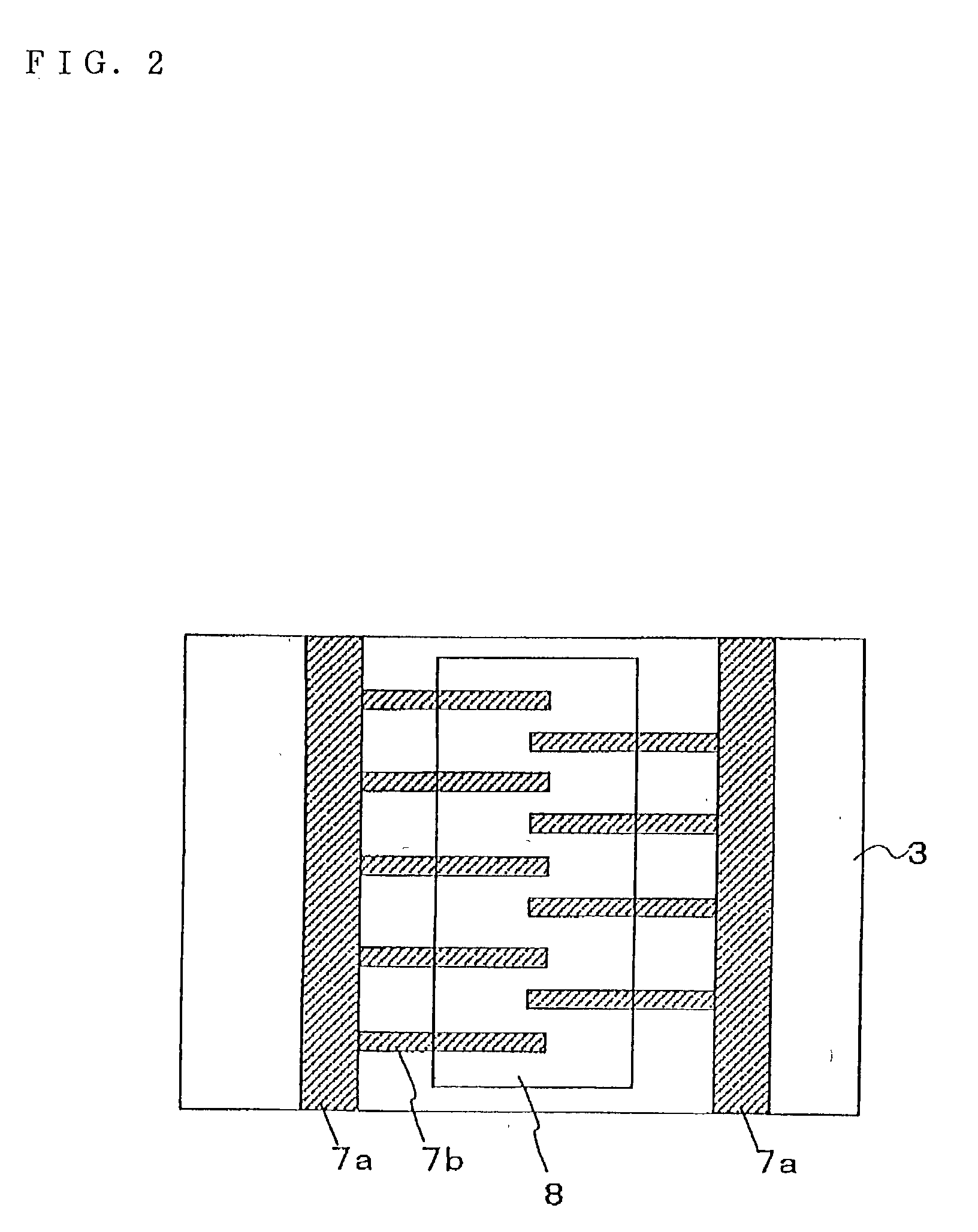
[0071] In this example, various patterns of copper interconnects extending in two or more directions (FIG. 8) were prepared and each pattern was evaluated for a reduction rate of a copper interconnect thickness in chips from its wafer center and periphery. FIG. 8 is a plan view illustrating the evaluated patterns, where the black areas are interconnects and numeric values are interconnect occupancies.

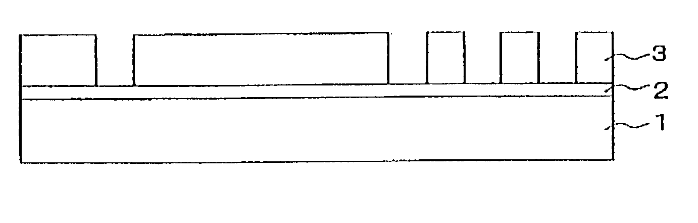
[0072] Copper interconnects were formed as illustrated in FIG. 6. As illustrated in FIG. 6(a), on a silicon substrate 1 are sequentially formed a silicon nitride film 2 with a thickness of 100 nm and a silicon oxide film 3 with a thickness of 1000 nm, and then a plurality of concaves reaching the silicon nitride film 2 were formed by dry etching in the silicon oxide film 3.

[0073] Subsequently, as illustrated in FIG. 6(b), on the whole surface was deposited a barrier metal film 4 consisting of Ta and TaN with a thickness of 15 nm by spattering. On the surface was then deposited by spatte...

example 2

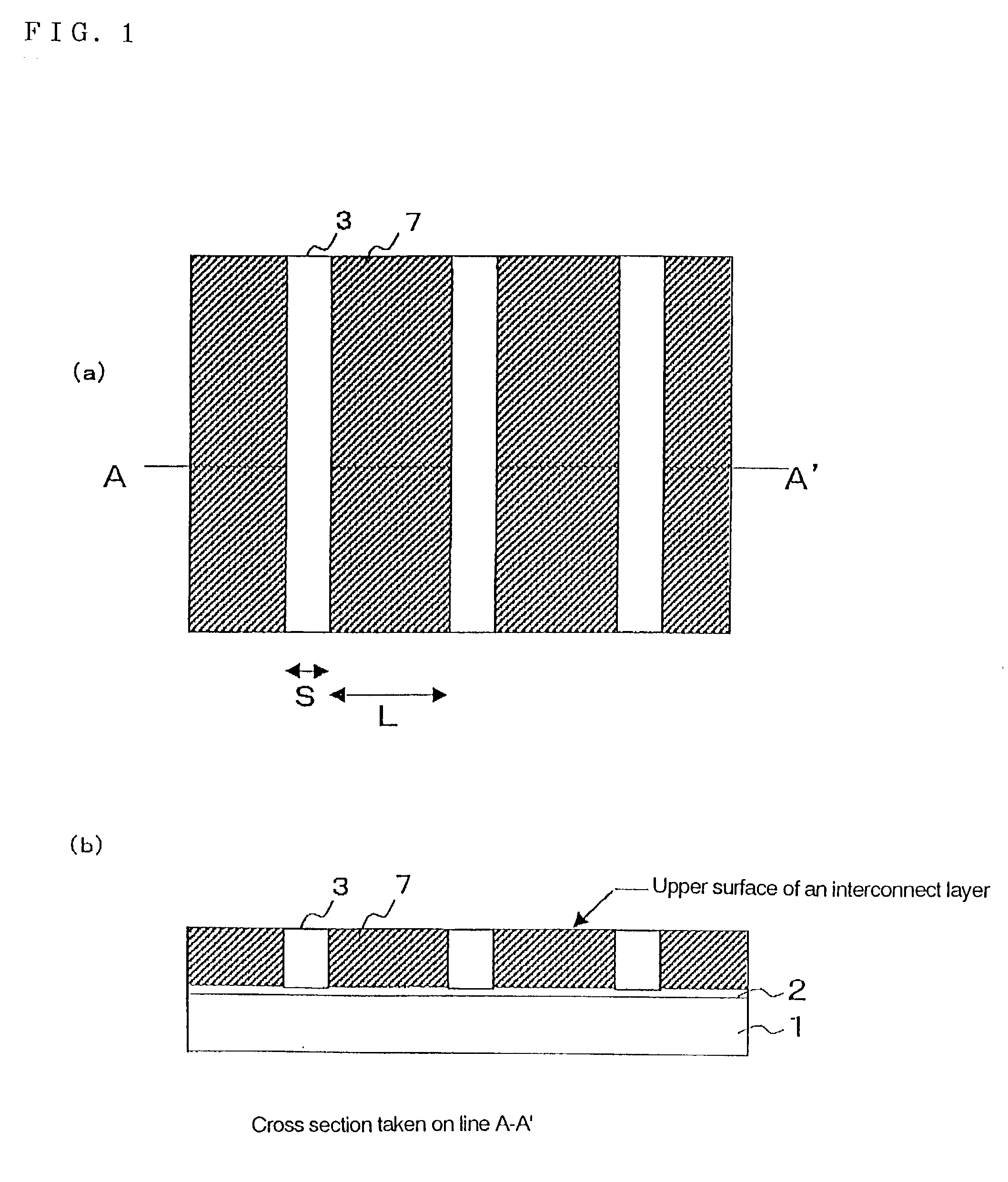
[0078] In this example, various patterns of copper interconnects comprising, as a main area, an area where copper interconnects extended over 100 .mu.m or more in one direction were prepared and each pattern was evaluated for a reduction rate of a copper interconnect thickness in chips from its wafer center and periphery. Each pattern has a unique L / S value where L is an interconnect width and S is a distance between adjacent interconnects.

[0079] The copper interconnects were prepared as described in Example 1, except changing an interconnect pattern. As with Example 1, the thickness of the copper interconnects was 300 nm.

[0080] After preparing the copper interconnects, a sheet resistance was determined for each pattern. A line / space ratio is shown in each figure. For example, "4 / 0.84" in FIG. 10 indicates that an interconnect width (line) is 4.mu.m and a distance between adjacent interconnects (space) is 0.84 .mu.m.

[0081] A sheet resistance was determined by a two-probe or four-pro...

example 3

[0086] On a semiconductor device was formed an MOSFET, on which were then deposited five interconnect layers, to prepare a logic IC. Table 2 shows a profile for each interconnect layer.

2 TABLE 2 Thickness L / S of copper (line / space interconnects ratio) Interconnect occupancy for the (nm) in area (a) whole interconnect layer (%) Lowest layer 30 10 / 3 (3.3) 55 2nd layer 30 10 / 3 (3.3) 55 3rd layer 30 10 / 3 (3.3) 55 4th layer 30 10 / 3 (3.3) 55 5th layer 60 20 / 7 (2.9) 75

[0087] The prepared IC exhibited excellent high-speed operability. In particular, the copper interconnects were made with a designed thickness; matching properties in operation with a high frequency circuit were satisfactory; and an yield was improved.

[0088] As described above, in this invention, an interconnect occupancy and a line / space ratio are adjusted to appropriate ranges. It can, therefore, effectively prevent dishing and erosion, as well as increase and dispersion in an interconnect resistance.


PUM


Abstract

There is disclosed a semiconductor device comprising a copper interconnect layer 7 where a copper film is buried in a concave in an insulating film 3 via a barrier metal film, wherein the copper interconnect layer 7 has a line/space ratio of 4.5 or less and an interconnect occupancy of 10 to 60%. It can effectively prevent dishing and erosion, as well as increase and dispersion in an interconnect resistance when forming damascene copper interconnects.

Description

[0001] 1. Field of the Invention[0002] This invention relates to a semiconductor device comprising copper interconnects and a manufacturing process therefor.[0003] 2. Description of the Prior Art[0004] Recent higher integration in a semiconductor device has increasingly required an interconnect layer having a lower resistance. Copper which is highly resistant to electromigration has been, therefore, widely used as an interconnect material. Copper as an interconnect material cannot be, however, anisotropically etched by RIE (Reactive Ion Etching), and thus is generally subject to a damascene process employing CMP (Chemical Mechanical Polishing). A conventional process for forming copper interconnects using CMP will be described with reference to FIG. 16.[0005] As illustrated in FIG. 16(a), on a silicon substrate 1 are sequentially formed a silicon nitride film 2 with a thickness of 100 nm and a silicon oxide film 3 with a thickness of 1000 nm. Then, in the silicon oxide film 3 are fo...

Claims


Application Information

Patent Timeline
IPC IPC(8): H01L21/304H01L21/768H01L23/52H01L21/3205H01L23/532
CPCH01L21/7684H01L23/53238H01L23/5329H01L2924/0002H01L2924/00
Inventor MATSUBARA, YOSHIHISA
Owner NEC ELECTRONICS CORP
Why Eureka
Try Eureka