Electrode and device using the same

a technology of electrodes and electrodes, applied in the direction of discharge tube main electrodes, tubes with screens, transit-tube cathodes, etc., can solve the problems of high current operation and reliability of a device, low voltage operation and high current operation, etc., to achieve enhanced throughput, high power microwave output, and high resolution

Inactive Publication Date: 2004-03-04
SUGINO TAKASHI +1
View PDF5 Cites 17 Cited by
  • Summary
  • Abstract
  • Description
  • Claims
  • Application Information

AI Technical Summary

Benefits of technology

0017] If an electron-emitting device according to the present invention is used for an electron beam exposure, an electron beam exposure with high resolution and enhanced throughput can be realized.
0018] If an electron-emitting device according to the present invention is used for a microwave traveling-wave tube, high-power microwave output can be obtained.
0019] If an electron-emitting device according to the present invention is used for an image pickup device, clear images can be realized.
0020] If an electron-emitting device according to the present invention is used for an electron beam source of a material evaluation device,

Problems solved by technology

However, low voltage operation, high current operation and reliability of a device have been required in the applications shown above.
However, there were problems about spatial stability in electron emission characteristics of these carbo

Method used


Image

  • Electrode and device using the same
  • Electrode and device using the same
  • Electrode and device using the same

Examples


embodiment 1

[0053] (Embodiment 1)

[0054] FIG. 1 is a schematic cross-sectional view of a first embodiment of an electron-emitting device according to the present invention. An electron-emitting device of embodiment 1 is composed of a substrate 1, a boron nitride thin film 2, a SiOx film 3, an extraction electrode 4, an anode electrode 5, a power source 6, 7, a cathode electrode 8.

[0055] In this embodiment, silicon was used for the substrate 1. On the substrate, 10 nm of the boron nitride thin film 2 was deposited by the plasma chemical vapor deposition (CVD) method using boron trichloride and nitrogen gas. Next, sulfur atoms were added to the boron nitride thin film 2 by concentration of 1.times.10.sup.18 cm.sup.-3. Further, 800 nm of the SiOx thin film 3 and Ti (20 nm) / Au (500 nm) as a metal for the extraction electrode 4 were formed on the boron nitride thin film 2 by the electron-beam evaporation method. Still further, AL (500 nm) as the cathode electrode 8 was electron-beam evaporated on the...

embodiment 2

[0060] (Embodiment 2)

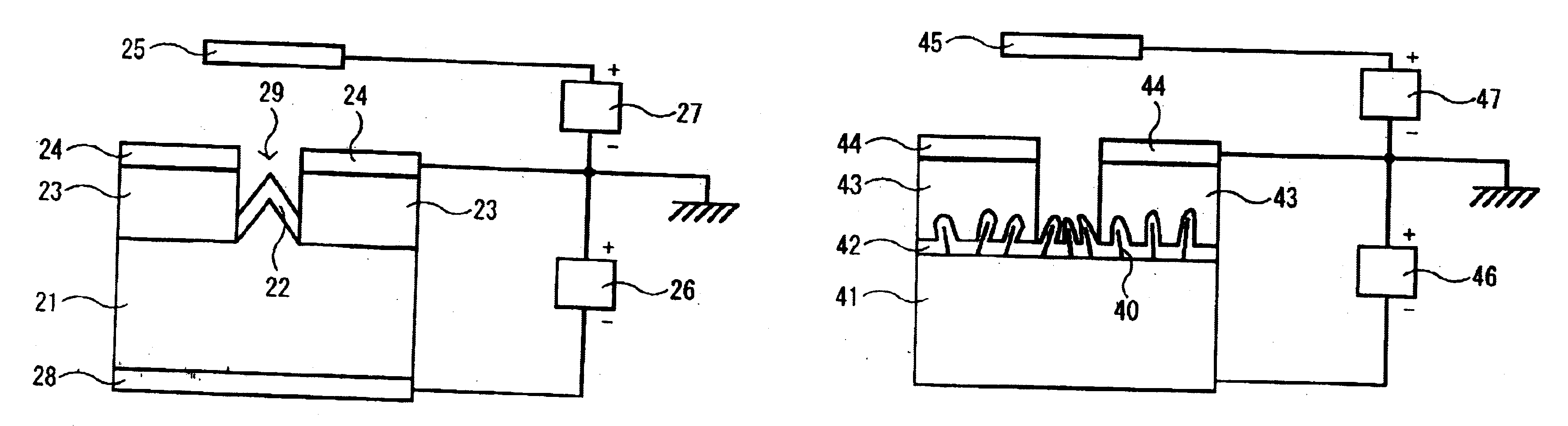
[0061] FIG. 2 is a schematic cross-sectional view of a second embodiment of an electron-emitting device according to the present invention. The electron-emitting device formed a spint-type spire shape on the silicon substrate 1 provided with the boron nitride carbon film of the present invention is composed of a substrate 21, a boron nitride carbon thin film 22, a SiOx film 23, an extraction electrode 24, an anode electrode 25, a power source 26, 27, a cathode electrode 28 and a spire shape 29.

[0062] The boron nitride carbon thin film 22 according to the present invention is formed at the spire shape 29 using an n-type silicon substrate 1 (111) on which the spire shape part 29 having the electrode 24. A 10 nm of the boron nitride carbon thin film 22 (composition ratio, boron 0.4, carbon 0.2, nitrogen 0.4) was deposited using boron trichloride, methane and nitrogen gas by the plasma assist chemical vapor deposition method. Sulfur atoms were added to the boron nit...

embodiment 3

[0064] (Embodiment 3)

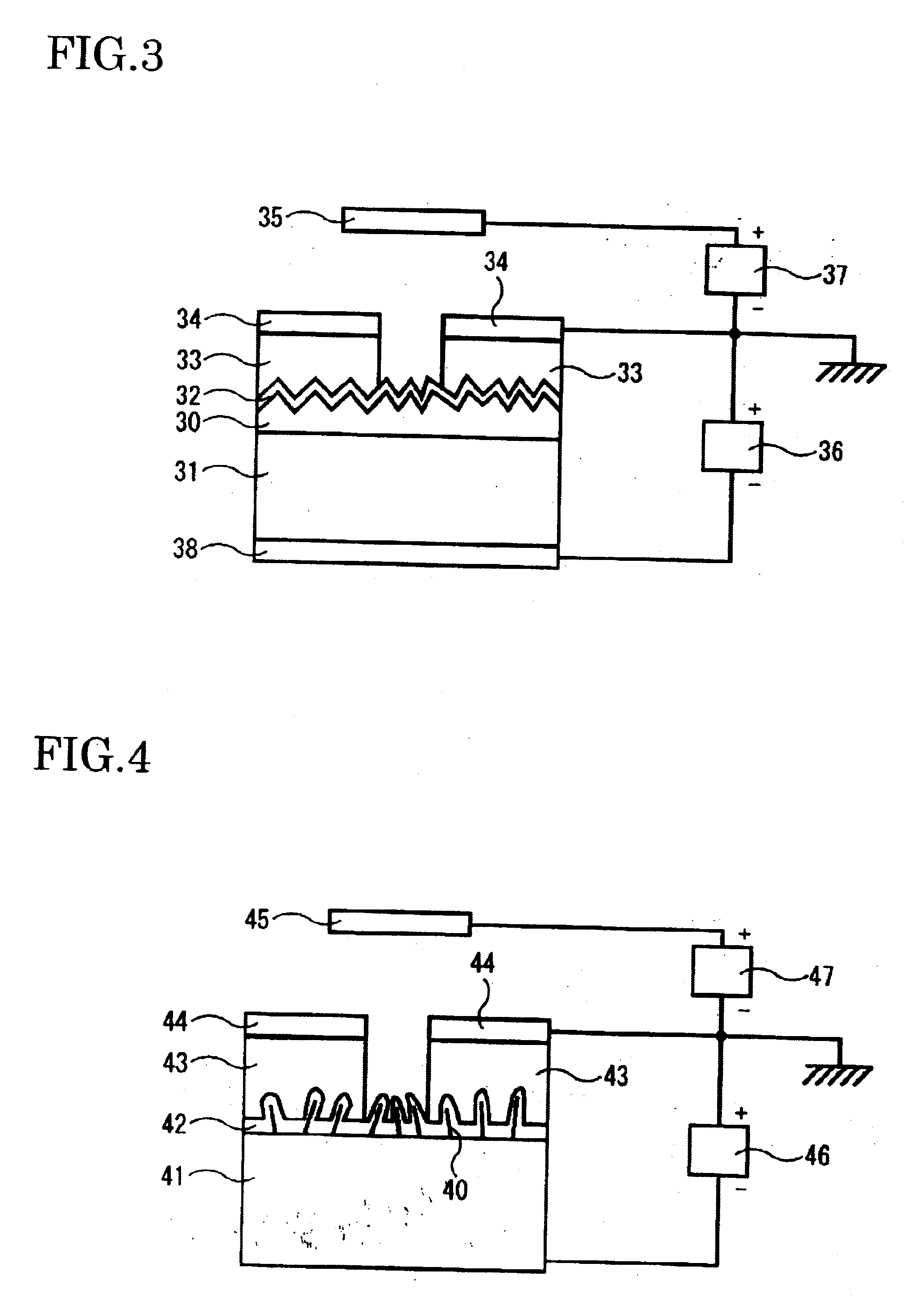
[0065] FIG. 3 is a schematic cross-sectional view of a third embodiment of an electron-emitting device according to the present invention. An electron-emitting device of embodiment 3 is composed of a substrate 31 onto which an n-type gallium nitride layer 30 is formed, boron nitride carbon thin film 32, SiOx film 33, extraction electrode 34, anode electrode 35, power source 36, 37, cathode electrode 38.

[0066] A wafer wherein the n-type gallium nitride layer 30 added silicon was grown by 1 .mu.m on the n-type silicon substrate 31 (111) by the metal organic chemical vapor deposition was used as a substrate. Hydrogen plasma is generated by microwave to process a surface of the gallium nitride layer 30. Processing was performed for five minutes by setting a microwave output to 300W, hydrogen flow to 50 sccm and gas pressure to 40 Torr. A flat surface of the gallium nitride layer 30 changes into a surface with irregularities of several decades nm. A 10 nm of the boro...


PUM


Abstract

A high-efficiency electron-emitting device that can emit electron with higher luminance at a voltage lower than conventional electron-emitting devices, as a key device of a flat panel display, image pickup device, electron beam device, microwave traveling-wave tube is provided to improve the carrier injection efficiency and enhance luminance of an organic light-emitting device. A film having space charge with a thickness of 50 nm or less is formed on a surface of a conductive material on which irregularities, amorphous or fibrous materials are formed. The film includes compounds of group 3 atoms such as aluminum nitride, boron nitride, aluminum nitride boron, aluminum nitride gallium, boron nitride gallium and nitrogen atoms, and nitride, carbon, silicon, oxygen and boron such as oxides including nitrogen boron carbon, boron carbide, carbon nitride, boron.

Description

[0001] 1. Technical Field[0002] The present invention relates to an electrode to inject and emit carrier effectively and a device using the same.[0003] 2. Background Art[0004] A cold cathode can be applied to a field emission display, electron beam exposure, microwave traveling wave tube, image pickup device and so on. It can be also used as an electrode source of a material evaluation device such as an Auger electron spectroscopy using electron beam. Further, it can be used as a light-emitting element for an illumination device or an indicator lamp and other varied applications.[0005] With regard to a cold cathode, an electron-emitting device called spint-type forming a spire using a metal or silicon has been researched and developed. However, low voltage operation, high current operation and reliability of a device have been required in the applications shown above. Under such circumstances, improvement of characteristics of a spint-type cold cathode and new materials for cold cat...

Claims


Application Information

Patent Timeline
IPC IPC(8): H01L51/50B82Y20/00B82Y99/00H01J1/304H01J11/22H01J11/34H01J23/04H01J29/04H01J31/12H01J37/073H01J63/06H05B33/26
CPCH01J2201/30426H01J1/304
Inventor SUGINO, TAKASHIKUSUHARA, MASAKIUMEDA, MASARU
Owner SUGINO TAKASHI
Why Eureka
Try Eureka