Resist material and nanofabrication method

a technology of resist material and nanofabrication method, which is applied in the direction of auxillary/base layers of photosensitive materials, instruments, photosensitive materials, etc., can solve the problems of metals, however, that present difficulties in nanofabrication by ultraviolet or visible light exposure, and achieve high-precision nanofabrication, high drawing speed, and reduced exposure time

Inactive Publication Date: 2004-09-02
SONY CORP
View PDF1 Cites 30 Cited by
  • Summary
  • Abstract
  • Description
  • Claims
  • Application Information

AI Technical Summary

Benefits of technology

0090] The nanofabrication method of the present invention, as described above, uses resist materials of the above incompletely oxidized transition metals. This results in the advantage that exposure can be carried out by a combination of an inorganic resist and ultraviolet or visible light. These inorganic resists are quite different from conventional ones in that the conventional inorganic resists cannot be combined with ultraviolet or visible light as an exposure source because the conventional inorganic resists are optically transparent to ultraviolet or visible light, and therefore require an expensive exposure apparatus such as an electron beam or ion beam apparatus.
0091] Moreover, the nanofabrication method uses ultraviolet or visible light having a high drawing speed to greatly reduce the time required for exposure as compared to nanofabrication methods using the conventional inorganic resists and electron beams.
0092] Furthermore, the nanofabrication method uses the inorganic resist materials of incompletely oxidized transition metals to provide a clear pattern at the boundary between exposed and unexposed areas, thereby achieving highprecision nanofabrication. In addition to this, in exposure, the nanofabrication method permits focusing by an exposure source itself, leading to high resolution.
0093] To form a fine pattern, as described above, the nanofabrication method of the present invention employs an approach to decrease the proportional constant K in the relation represented by P=K.multidot..lambda. / NA. This approach is different from the conventional approach to achieve nanofabrication at a shorter exposure wavelength .lambda. and a larger numerical aperture NA of the objective lens. This approach allows formation of a finer pattern using exposure apparatuses currently in use. Specifically, the present invention allows the proportional constant K to be below 0.8 and the minimum nanofabrication cycle f of a workpiece to be reduced as follows:
0094] The present invention, therefore, achieves the provision of inexpensive devices allowing direct use of exposure apparatuses currently in use as well as finer processing.

Problems solved by technology

These metals, however, present difficulty in nanofabrication by exposure with ultraviolet or visible light because these metals are transparent to ultraviolet or visible light to exhibit significantly low absorption.

Method used


Image

  • Resist material and nanofabrication method
  • Resist material and nanofabrication method
  • Resist material and nanofabrication method

Examples


example 1

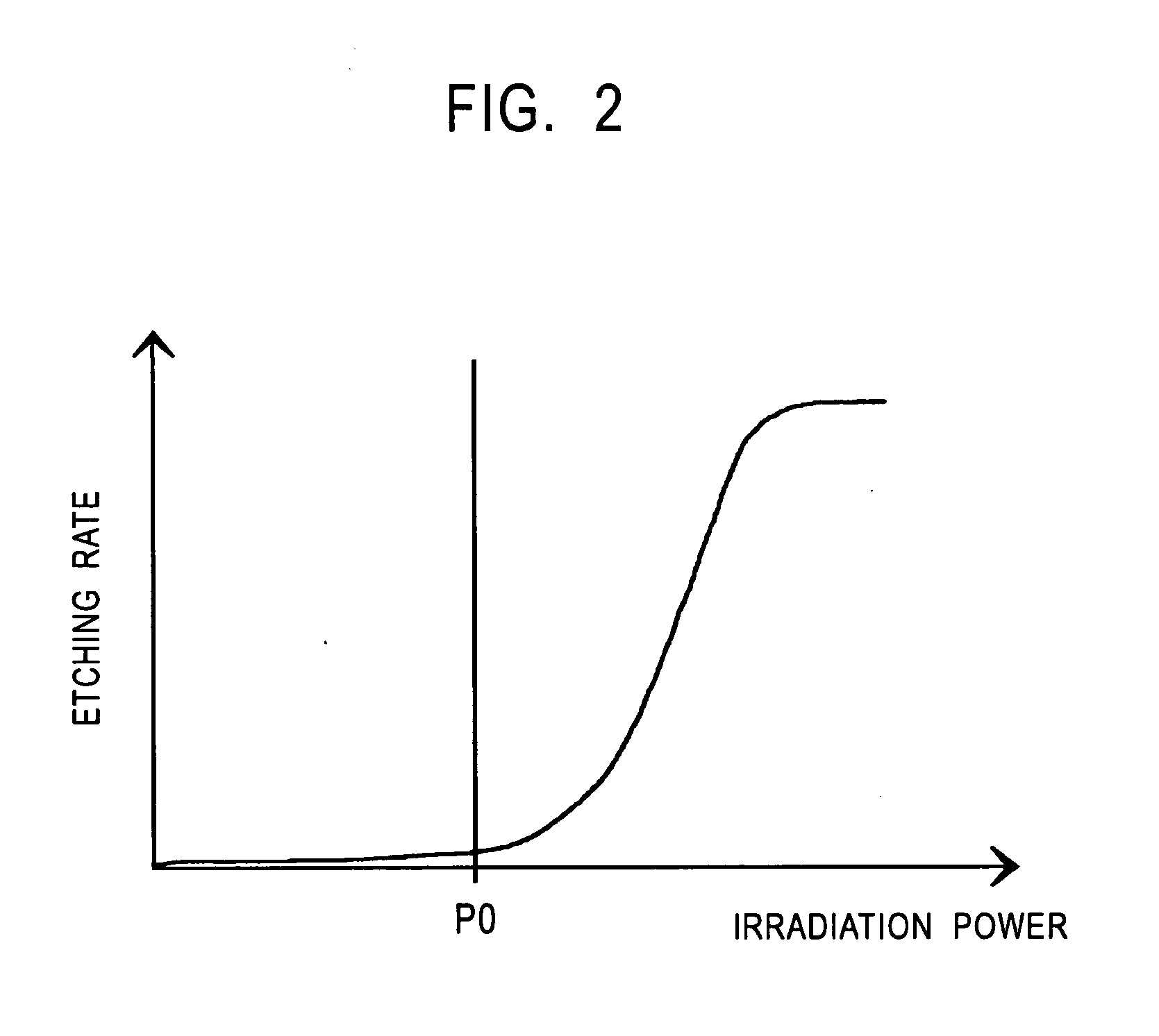
[0096] In Example 1, a resist master for optical discs was prepared with incompletely oxidized trivalent tungsten as a resist material.

[0097] A resist layer of incompletely oxidized tungsten was uniformly deposited on a glass substrate having a sufficiently smooth surface by sputtering. The sputtering was carried out with elemental tungsten as a sputtering target in an argon-oxygen mixed atmosphere, of which the oxygen gas concentration was changed to control the degree of oxidation of the incompletely oxidized tungsten.

[0098] The deposited resist layer was analyzed with an energy dispersive X-ray spectrometer (EDX) to give x=0.63 in terms of composition W.sub.1-xO.sub.x, wherein the resist layer was 40 nm thick; and the dependence of the refractive index on the wavelength was measured by spectroellipsometry.

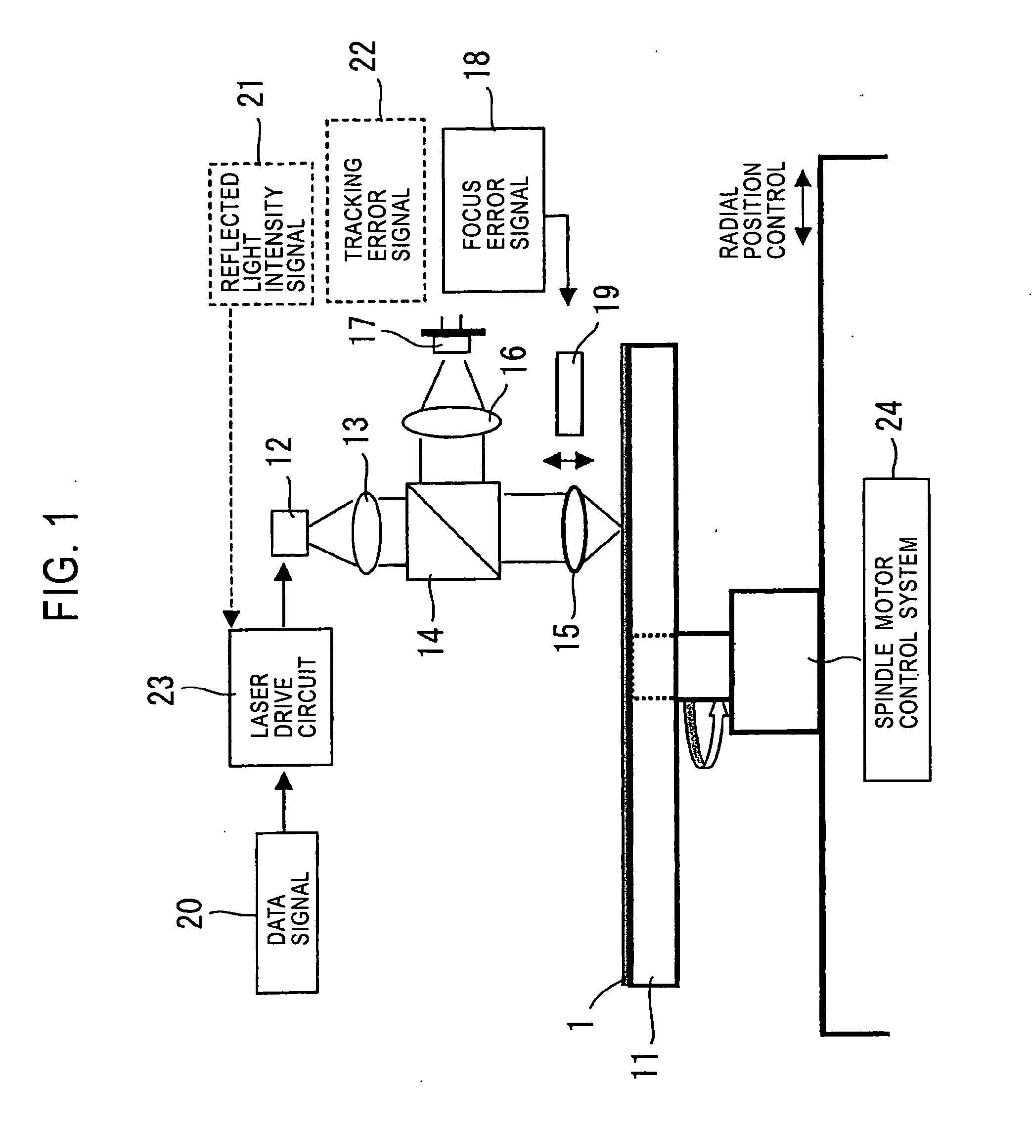
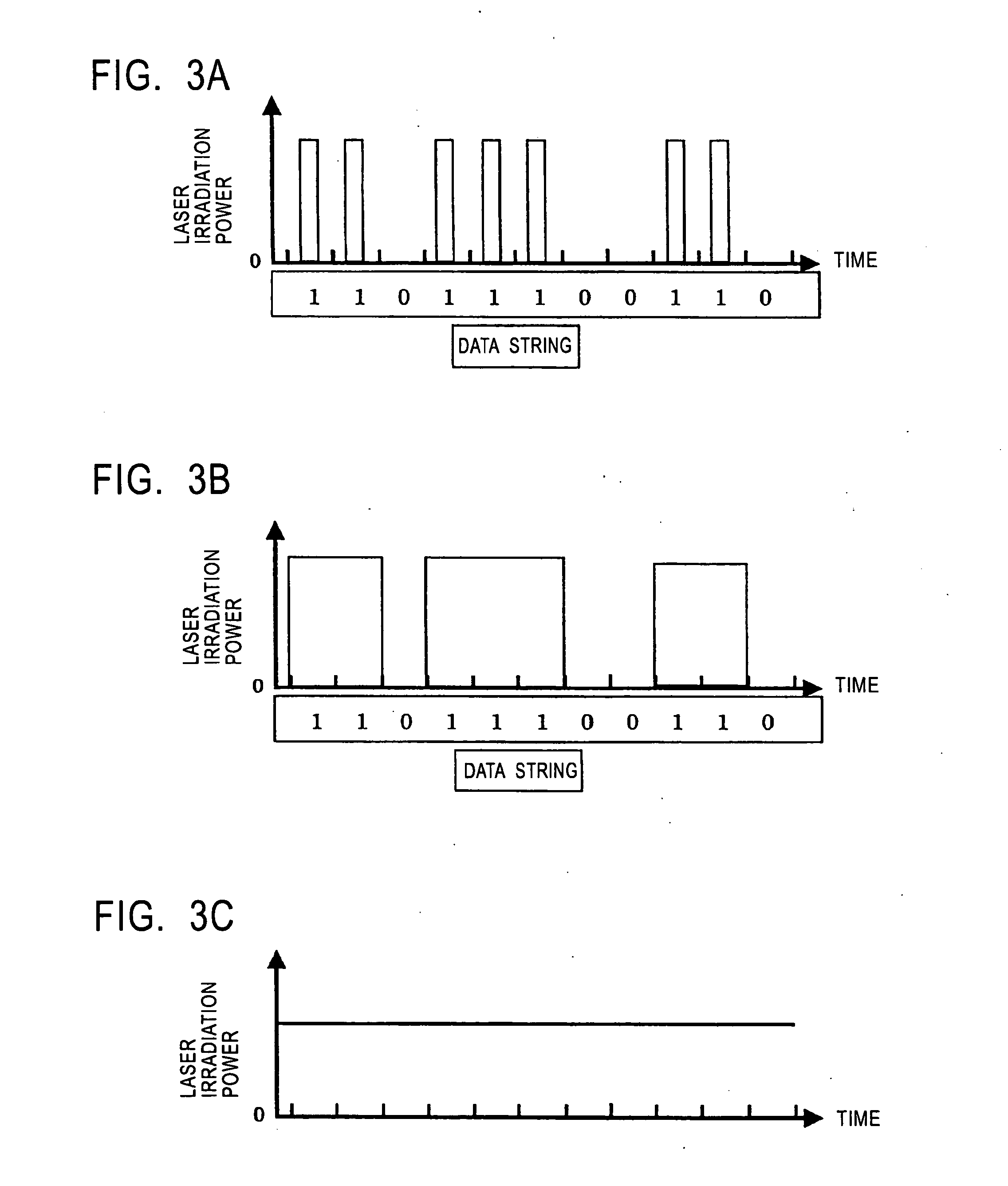
[0099] The substrate covered with the resist layer was disposed on the turntable in the exposure apparatus shown in FIG. 1. The resist layer was irradiated with a laser having a...

example 2

[0105] In Example 2, a resist master for optical discs was prepared with incompletely oxidized trivalent molybdenum as a resist material.

[0106] Example 2 employed nearly the same process as Example 1 except that molybdenum was used as a sputtering target. Through the process, a resist layer of incompletely oxidized molybdenum was deposited on a glass substrate, was exposed, and was developed to form pits, as shown in FIG. 6. The deposited resist layer was analyzed with an EDX to give x=0.59 in terms of composition Mo.sub.1-xO.sub.x.

[0107] In contrast with incompletely oxidized tungsten, the resist layer of the incompletely oxidized molybdenum forms pits at exposed areas, which are convex with respect to an unexposed area, as shown in FIG. 6. This is because the incompletely oxidized molybdenum functions as a negative resist to the tetramethylammonium hydroxide solution.

example 3

[0114] In Example 3, a resist master for optical discs was prepared with incompletely oxidized trivalent tungsten and molybdenum as resist materials, and an optical disc was finally prepared. FIG. 7 shows an outline of the preparation process.

[0115] An amorphous silicon intermediate layer 101 having a thickness of 80 nm was uniformly deposited on a substrate 100 of a silicon wafer by sputtering. A resist layer 102 of incompletely oxidized tungsten and molybdenum was further uniformly deposited on the substrate 100 by sputtering (FIG. 7(a)). The sputtering was performed in an argon atmosphere with a sputtering target of incompletely oxidized tungsten and molybdenum. The deposited resist layer was analyzed with an EDX to give 80:20 in the ratio of tungsten to molybdenum contained in the deposited incompletely oxidized tungsten and molybdenum, and 60 atomic percent in oxygen content. The resist layer had a thickness of 55 nm. Electron diffraction analysis by a transmission electron mic...


PUM

PropertyMeasurementUnit
wavelengthaaaaaaaaaa
pit lengthaaaaaaaaaa

Abstract

A resist material and a nanofabrication method provide high-resolution nanofabrication without an expensive irradiation apparatus using, for example, electron beams or ion beams. That is, the resist material and the nanofabrication method provide finer processing using exposure apparatuses currently in use. A resist layer of an incompletely oxidized transition metal such as W and Mo is selectively exposed and developed to be patterned in a predetermined form. The incompletely oxidized transition metal herein is a compound having an oxygen content slightly deviated to a lower content from the stoichiometric oxygen content corresponding to a possible valence of the transition metal. In other words, the compound has an oxygen content lower than the stoichiometric oxygen content corresponding to a possible valence of the transition metal.

Description

[0001] The present invention relates to inorganic resist materials and nanofabrication methods with the resist materials and, particularly, to a resist material and a nanofabrication method allowing high-precision nanofabrication with an exposure source over ultraviolet to visible light region.[0002] The latest lithography for nanofabrication in, for example, semiconductors, optical devices, and magnetic devices requires patterning precision on the order of tens of nanometers or less. To achieve such high-precision patterning, intensive development has been made in various fields such as light sources, resist materials, and steppers.[0003] Effective approaches to enhance the dimensional precision of nanofabrication include use of shorter wavelengths and convergent electron or ion beams in an exposure source. However, short-wavelength exposure sources and convergent electron or ion beam irradiation sources are so expensive that these sources are unsuitable for providing less expensiv...

Claims


Application Information

Patent Timeline
Patent Type & Authority Applications(United States)
IPC IPC(8): G03F7/004G03F7/16G11B7/26H01L21/027
CPCB82Y10/00G11B7/261G03F7/0043G03F7/004
Inventor KOUCHIYAMA, AKIRAARATANI, KATSUHISA
Owner SONY CORP
Why Eureka
Try Eureka