Boron phosphide-based semiconductor device and production method thereof

a technology of boron phosphide and semiconductors, which is applied in the direction of polycrystalline material growth, natural mineral layered products, crystal growth process, etc., can solve the problems of unclarified boron vacancy and the p-type conduction of the bp layer not always stably obtained, so as to increase the amount of donor-related anti-site defects and achieve stably obtained

Inactive Publication Date: 2004-11-25
SHOWA DENKO KK
View PDF1 Cites 4 Cited by
  • Summary
  • Abstract
  • Description
  • Claims
  • Application Information

AI Technical Summary

Benefits of technology

0034] In the condition where phosphorus vacancy is already present in excess of the concentration of boron vacancy in the undoped state, in other words, boron atom occupying the phosphorus vacancy, acting as an acceptor, is present in a large amount, even if an n-type impurity is added, the entire amount cannot be electrically compensated and a p-type layer containing residual acceptor components may be disadvantageously formed or only a high-resistance layer is obtained. When a condition in which the boron vacancy is present in a concentration higher than the phosphorus vacancy is created in the undoped state as in the present invention, the majority of n-type impurity added can act as an electrically active donor, though a part of the n-type impurity is consumed to form a donor/acceptor pair with the acceptor. Accordingly, in such a condition, an advantage is given that an n-type boron phosphide-based semiconductor layer having a controlled resistivity can be stably obtained by increasing or decreasing the amount of n-type impurity added

Problems solved by technology

For example, in the state in which phosphorus occupying the vacant lattice point of boron, which is considered to act as a donor, is present in a large amount, even if a p-type impurity is doped, a BP layer showing p-type conduction is not always stably obtained.
Moreover, the effect given by the addition of a p-type or n-type impu

Method used


Image

  • Boron phosphide-based semiconductor device and production method thereof
  • Boron phosphide-based semiconductor device and production method thereof
  • Boron phosphide-based semiconductor device and production method thereof

Examples


Embodiment Construction

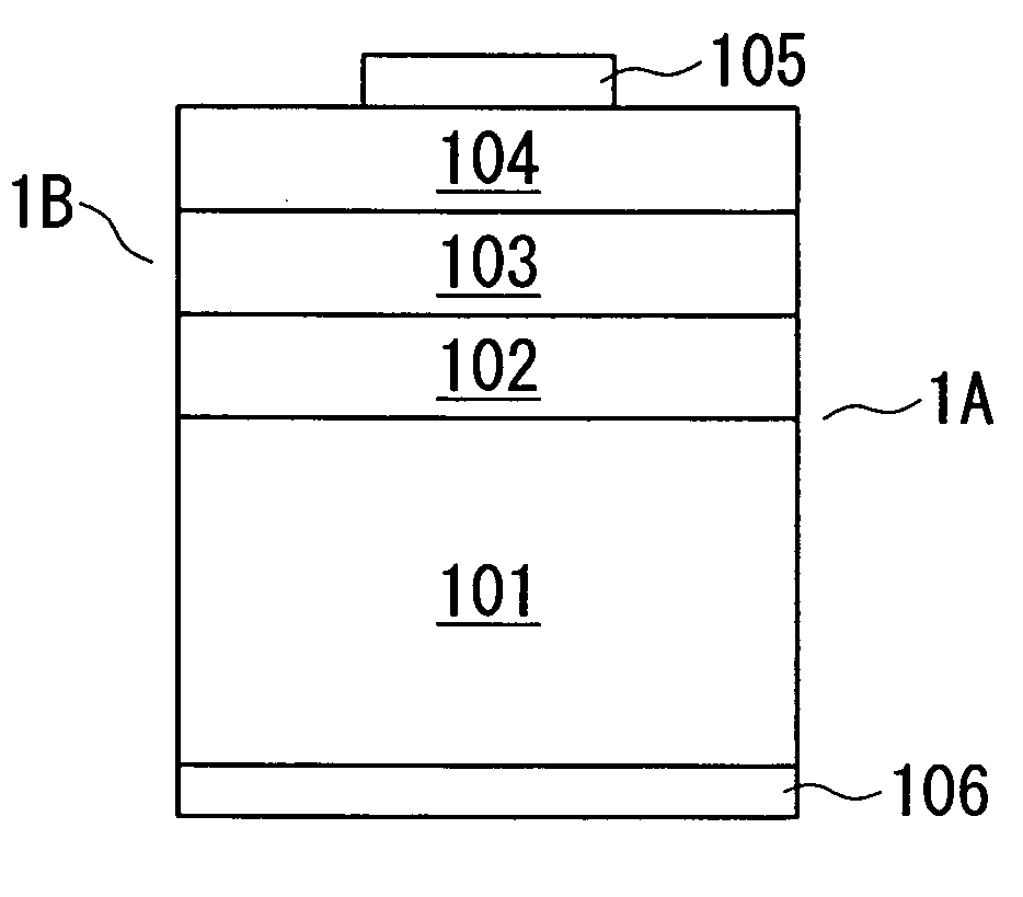
[0042] The present invention is specifically described below by referring to the case where a boron phosphide-based semiconductor light-emitting diode (LED) is fabricated by utilizing p-type and n-type boron phosphide (BP) semiconductor layers provided on a silicon single crystal substrate.

[0043] FIG. 1 is a view schematically showing the cross section of LED 1B according to this Example. For the single crystal substrate 101, a boron (B)-doped p-type silicon single crystal with the (111) crystal plane surface was used. On the substrate 101 surface, a lower clad layer 102 composed of a zinc (Zn)-doped (111) p-type boron phosphide (BP) was formed at 1,050.degree. C. by an atmospheric pressure MOCVD method using a triethylborane ((C.sub.2H.sub.5).sub.3B) / phosphine (PH.sub.3) / hydrogen (H.sub.2) system. At the formation, the V / III ratio (.dbd.PH.sub.3 / (C.sub.2H.sub.5).sub.3B feed ratio) was set to about 115. By the analysis using a laser Raman spectroscopic method or the like, the concen...


PUM

PropertyMeasurementUnit
Angleaaaaaaaaaa
Angleaaaaaaaaaa
Temperatureaaaaaaaaaa

Abstract

A boron phosphide-based semiconductor device includes a single crystal substrate having formed thereon a boron-phosphide (BP)-based semiconductor layer containing boron and phosphorus as constituent elements, where phosphorus (P) occupying the vacant lattice point (vacancy) of boron (B) and boron occupying the vacant lattice point (vacancy) of phosphorus are present in the boron-phosphide (BP)-based semiconductor layer. The boron phosphide-based semiconductor device includes a p-type boron phosphide-based semiconductor layer in which boron occupying the vacancy of phosphorus is contained in a higher atomic concentration than phosphorus occupying the vacancy of boron and a p-type impurity of Group II element or Group IV element is added.

Description

[0001] This application claims the benefit pursuant to 35 U.S.C. .sctn.119(e)(1) of U.S. Provisional Application No. 60 / 343,233 filed Dec. 31, 2001.[0002] The present invention relates to a technique for fabricating a boron phosphide-based compound semiconductor device by utilizing a boron phosphide-based semiconductor layer having p-type or n-type electrical conductivity or high resistance.[0003] Boron phosphide (BP) is conventionally known as one of Group III-V compound semiconductors (see, Iwao Teramoto, Handotai Device Gairon (Introduction to Semiconductor Devices), page 28, Baifukan (Mar. 30, 1995)). The boron phosphide is an almost covalent bonding semiconductor having a Phillips ionicity (=.delta.) as small as 0.006 (see, Phillips, Handotai Ketsugo Ron (Bonds and Bands in Semiconductors), 3rd imp., page 51, Yoshioka Shoten (Jul. 25, 1985)). Furthermore, the boron phosphide is a zinc-blend type cubic crystal (see, Handotai Device Gairon (Introduction of Semiconductor Device), ...

Claims


Application Information

Patent Timeline
IPC IPC(8): C30B25/02C30B29/40H01L21/205H01L29/201H01L29/207H01L33/30
CPCC30B25/02C30B29/40H01L21/02381H01L21/02461H01L21/0254H01L21/02543H01L21/02546H01L21/02576H01L21/02579H01L21/0262H01L29/201H01L29/207H01L33/30Y10S438/935H01L21/20
Inventor UDAGAWA, TAKASHI
Owner SHOWA DENKO KK
Why Eureka
Try Eureka