Polyelectrolyte nanolayers as diffusion barriers in semiconductor devices

a technology of polyelectrolyte nanolayers and semiconductor devices, applied in semiconductor devices, semiconductor/solid-state device details, electrical apparatus, etc., can solve the problems of increasing operating speed, shrinking dimensions, and copper diffusion rapidly in silicon, silicon dioxide and other low-k materials, and achieve the effect of improving the adhesion of the conductive layer to the substra

Active Publication Date: 2005-01-06
RENESSELAER POLYTECHNIC INST
View PDF11 Cites 21 Cited by
  • Summary
  • Abstract
  • Description
  • Claims
  • Application Information

AI Technical Summary

Benefits of technology

The present invention provides a diffusion barrier useful in an integrated circuit, which serves to prevent the migration of material from a conductive layer to the underlying substrate and further provides improved adhesion of the conductive layer to the substrate. The diffusion barrier comprises a polymer which is a polyelectrolyte, having both cationic and anionic groups along its backbone chain. Preferred polyelectolyte barriers are polyethyleneimine (PEI) and polyacrylic acid (PAA). Other polyelectrolytes may be used, such as those that contain SH—, OH—, aromatic groups, or those that can interact with either the metal or the adjacent layers via covalent interactions and cross-linking (e.g., POMA, polyoctadecene maleic anhydride, PSMA, polystyrene maleic anhydride, etc.). The polymeric layer may be applied in two coatings, so that the amine side chains contact the dielectric (e.g. silicon) substrate and the acidic groups are adjacent to the overlying metallic interconnect (e.g. copper). The diffusion barrier may be made thin, preferably less than 5 nm thick, which is advantageous in devices having high aspect ratios.

Problems solved by technology

Increasing demands are resulting in shrinking dimensions in order to accommodate more circuits on a chip, and increasing operating speeds, which approach the inherent delay in traditional semiconductor materials.
However, copper diffuses rapidly in silicon, silicon dioxide and other low k materials.
The diffusion, over time, through the dielectric material, results in junction linkage, which decreases device efficiency.
One of the challenges in Cu metallization technology is to prevent the rapid diffusion of Cu into SiO2 under an electrical bias during device operation.
This is because Cu incorporation degrades the dielectric properties of the oxide layer, causing leakage currents and leading to inferior device performance and failure.
While this approach has been successful thus far, new types of barriers are likely to be needed at device dimensions below 100 nm in contemporary device architectures, and very high-aspect ratio structures in 3D-integration of multiple-wafer devices.
This is difficult to achieve by conventional physical and chemical vapor deposition methods without compromising either conformal coverage of high aspect ratio features and / or the barrier layer microstructure, both of which reduce the efficacy of the barrier.
The formation of these layers, however, uses sophisticated sputtering processes and results in the inclusion of substantial contaminants.
2], formed by conventional vapor deposition methods, do not form uniform and continuous films at thicknesses below 10 nm, especially in non-planar topographies with high (e.g., 5:1) depth-to-width aspect ratios.
Furthermore, even if <5-nm-thick conformal films are achieved, it is not clear if conventional barrier materials will be effective at these thicknesses due to fast diffusion paths such as nanopipes [Ref.

Method used


Image

  • Polyelectrolyte nanolayers as diffusion barriers in semiconductor devices
  • Polyelectrolyte nanolayers as diffusion barriers in semiconductor devices
  • Polyelectrolyte nanolayers as diffusion barriers in semiconductor devices

Examples


examples

1. Substrates and Preparation

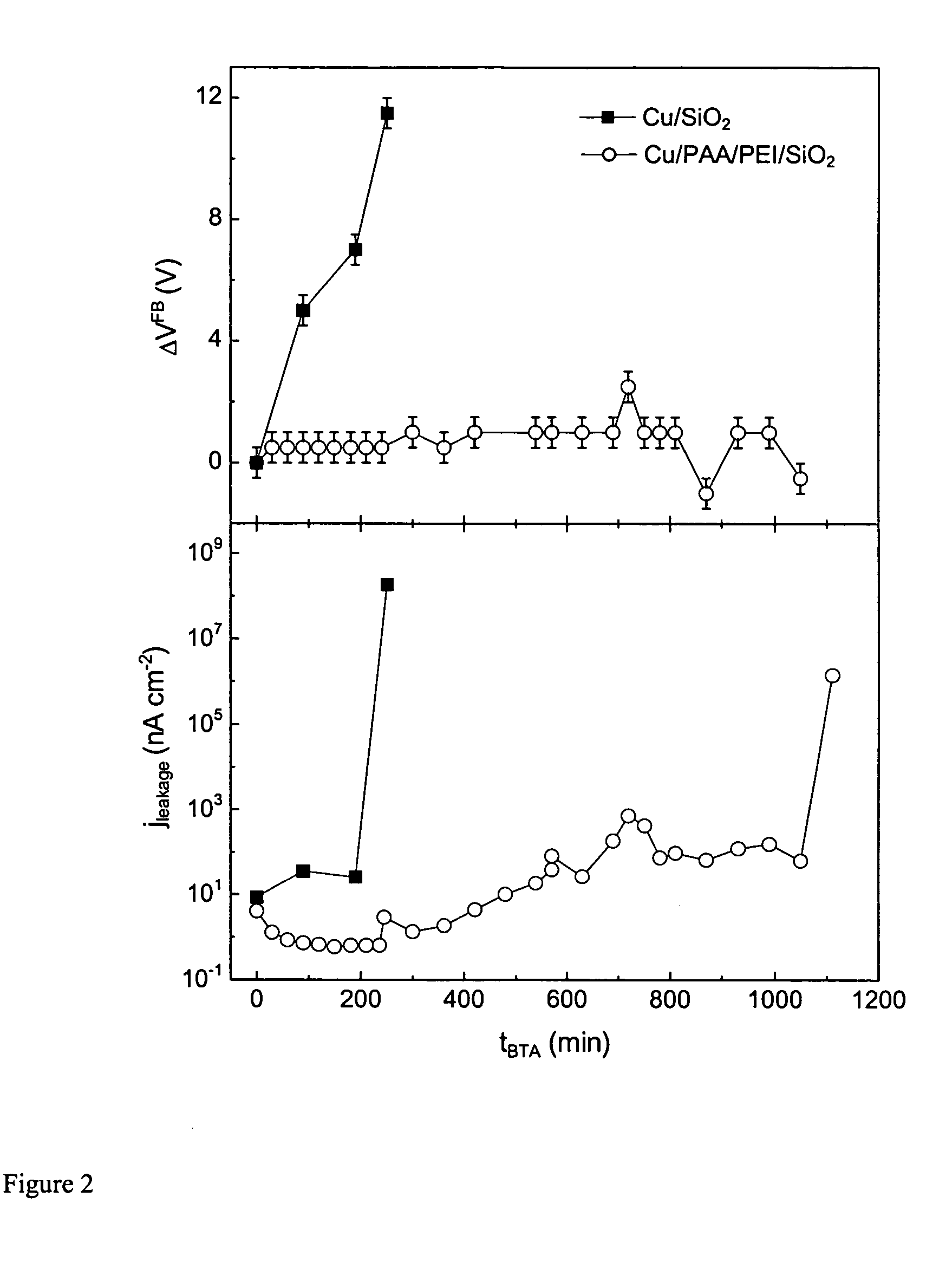
The substrates used with the present invention may be any low k semiconductor material. The work described below employed n-type device-quality Si(00) (i.e. a silicon wafer) capped with an 85-nm-thick dry thermal oxide. Each wafer was successively rinsed ultrasonically in acetone, methanol and DI water. A 500-nm-thick Al layer was sputter-deposited in a 5 mTorr Ar plasma after stripping the back oxide with HF, and annealed at 450 ° C. for 1 hour in a 10−6 Torr vacuum for ohmic contact formation.

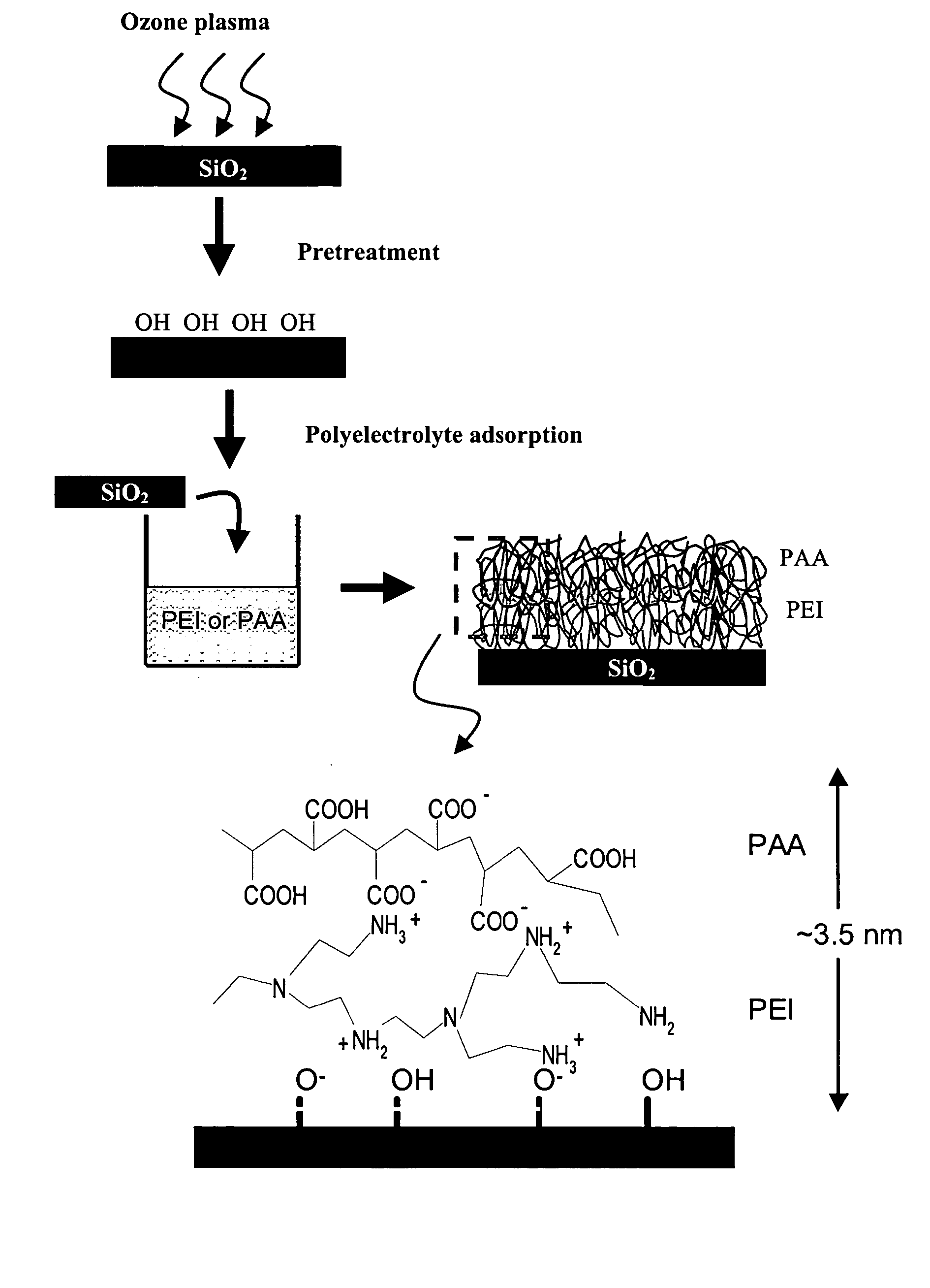
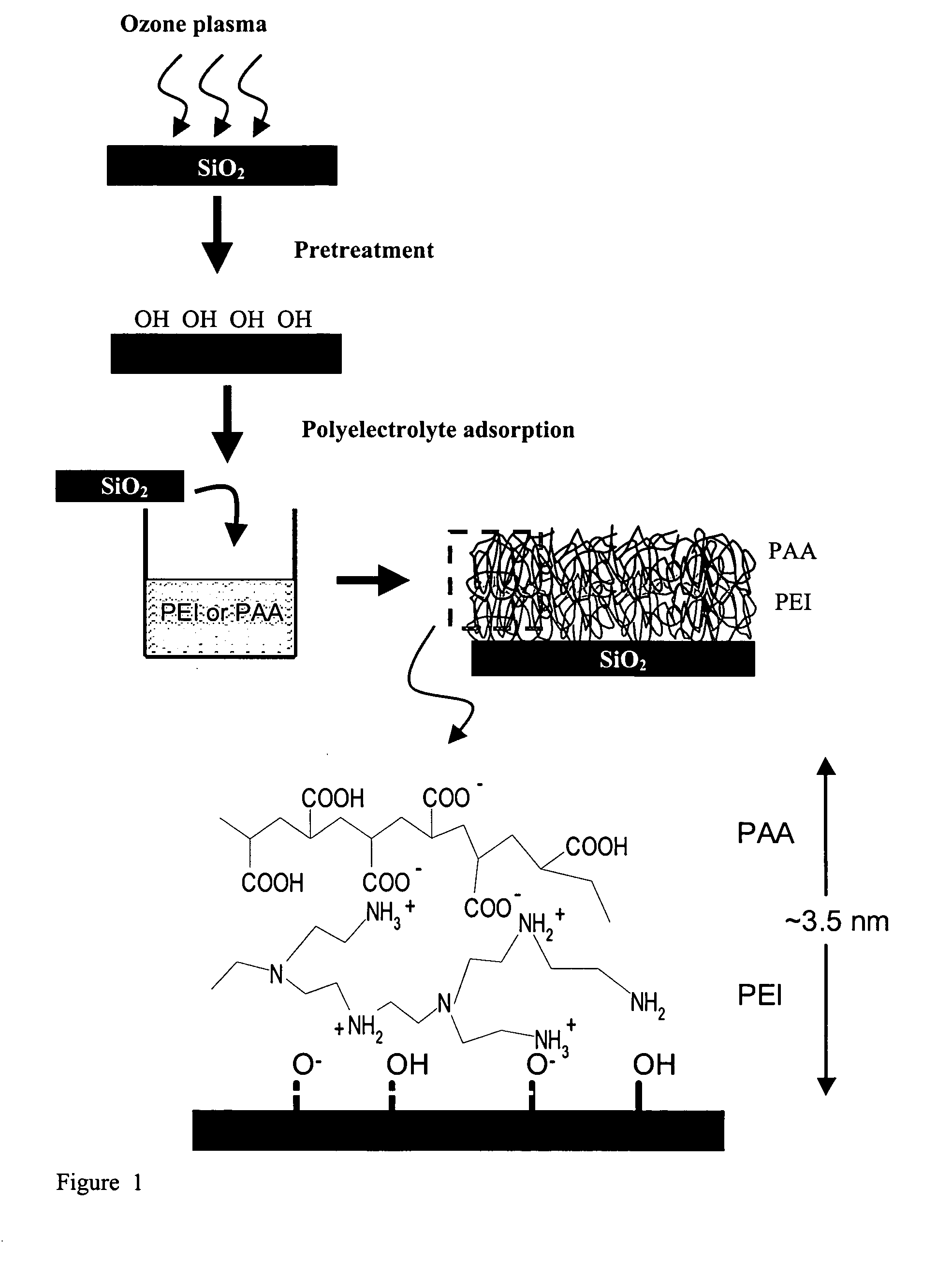
FIG. 1 shows a schematic diagram of the sample preparation procedure. The substrates were hydroxylated by exposure to an ozone plasma for 30 minutes at room tempearature to hydroxylate the substrate prior to polyelectrolyte adsorption.

The SiO2 coated, pre-treated substrate is subjected to coatings of polycationic PEI and polyanionic PAA. The adsorption of these layers onto the substrate results in a PEI layer immediately contacting the SiO2 and a PAA layer a...


PUM


Abstract

The present invention provides a diffusion barrier useful in an integrated circuit, which serves to prevent the migration of material from a conductive layer to the underlying substrate and further provides improved adhesion of the conductive layer to the substrate. The diffusion barrier comprises a polymer which is a polyelectrolyte, having both cationic and anionic groups along its backbone chain. Preferred polyelectolyte barriers are polyethyleneimine (PEI) and polyacrylic acid (PAA). Other polyelectrolytes may be used, such as those that contain SH— OH— aromatic groups, or those that can interact with either the metal or the adjacent layers via covalent interactions and cross-linking (e.g., POMA, PSMA). The polymeric layer may be applied in two coatings, so that the amine side chains contact the dielectric (e.g. silicon) substrate and the acidic groups are adjacent to the overlying metallic interconnect (e.g. copper). The diffusion barrier may be made thin, preferably less than 5 nm thick, which is advantageous in devices having high aspect ratios.

Description

REFERENCE TO A “SEQUENCE LISTING,” A TABLE, OR A COMPUTER PROGRAM LISTING APPENDIX SUBMITTED ON A COMPACT DISK Not Applicable BACKGROUND OF THE INVENTION A. Field of the Invention The present invention generally relates to integrated circuits. In particular, it relates to forming a diffusion barrier layer comprising a polyelectrolyte monolayer, bilayer, or multilayers in order to prevent diffusion of a metal interconnect (e.g. copper) into a semiconductor or insulating material (e.g. Si or SiO2). B. Description of Related Art In order to achieve the increasing demands for semiconductor performance, many new manufacturing techniques are being developed and introduced. Increasing demands are resulting in shrinking dimensions in order to accommodate more circuits on a chip, and increasing operating speeds, which approach the inherent delay in traditional semiconductor materials. Copper is the preferred metal for creating multilevel interconnect structures in ultra-large-scale-int...

Claims


Application Information

Patent Timeline
Patent Type & Authority Applications(United States)
IPC IPC(8): H01L21/288H01L21/312H01L21/3205H01L21/768H01L23/532
CPCH01L21/288H01L21/312H01L21/32051H01L21/76829H01L21/76832H01L21/76841H01L23/53238H01L2924/0002H01L23/5329H01L23/53295H01L2221/1078H01L2924/00H01L21/02118H01L21/02282
Inventor GANAPATHIRAMAN, RAMANATHKANE, RAVINDRA S.PETHURAJA, GOPAL GANESAN
Owner RENESSELAER POLYTECHNIC INST
Why Eureka
Try Eureka