Self-ionized and inductively-coupled plasma for sputtering and resputtering

a plasma and inductive coupling technology, applied in the direction of vacuum evaporation coating, electrolysis components, coatings, etc., can solve the problems of introducing reliability problems, difficult reflowing, and disadvantageous wide distribution

Inactive Publication Date: 2005-01-13
APPLIED MATERIALS INC
View PDF99 Cites 112 Cited by
  • Summary
  • Abstract
  • Description
  • Claims
  • Application Information

AI Technical Summary

Problems solved by technology

Lining and filling via holes and similar high aspect-ratio structures, such as occur in dual damascene, have presented a continuing challenge as their aspect ratios continue to increase.
Such a wide distribution can be disadvantageous for filling a deep and narrow via hole 122 such as that illustrated in FIG. 2, in which a barrier layer 124 has already been deposited.
Once a void 134 has formed, it is often difficult to reflow it out by heating the metallization to near its melting point.
Even a small void can introduce reliability problems.
If a second metallization deposition step is planned, such as by electroplating, the bridged overhang make subsequent deposition more difficult.
Both long-throw targets and collimators typically reduce the flux of sputter particles reaching the wafer and thus tend to reduce the sputter deposition rate.
Also, the length that long throw sputtering may be increased may be limited.
A yet further problem with both long throw and collimation is that the reduced metal flux can result in a longer deposition period which can not only reduce throughput, but also tends to increase the maximum temperature the wafer experiences during sputtering.
Still further, long throw sputtering can reduce over hangs and provide good coverage in the middle and upper portions of the sidewalls, but the lower sidewall and bottom coverage can be less than satisfactory.
If so, such a film may not promote hole filling, particularly when the liner is being used as the electrode for electroplating.
One of its fundamental problems is the limited number of variables available in optimizing the magnetic field configuration.
The horizontally arranged permanent magnets disclosed by Lai in U.S. Pat. No. 5,593,551 poorly address this effect.
However, CVD copper seed layers have often been observed to be rough.
However, complete fills performed by CVD can suffer from center seams, which may impact device reliability.
Hence, the CVD layer over an IMP layer will also tend to be rough.
Electroplating, however, imposes its own requirements.

Method used


Image

  • Self-ionized and inductively-coupled plasma for sputtering and resputtering
  • Self-ionized and inductively-coupled plasma for sputtering and resputtering
  • Self-ionized and inductively-coupled plasma for sputtering and resputtering

Examples


Embodiment Construction

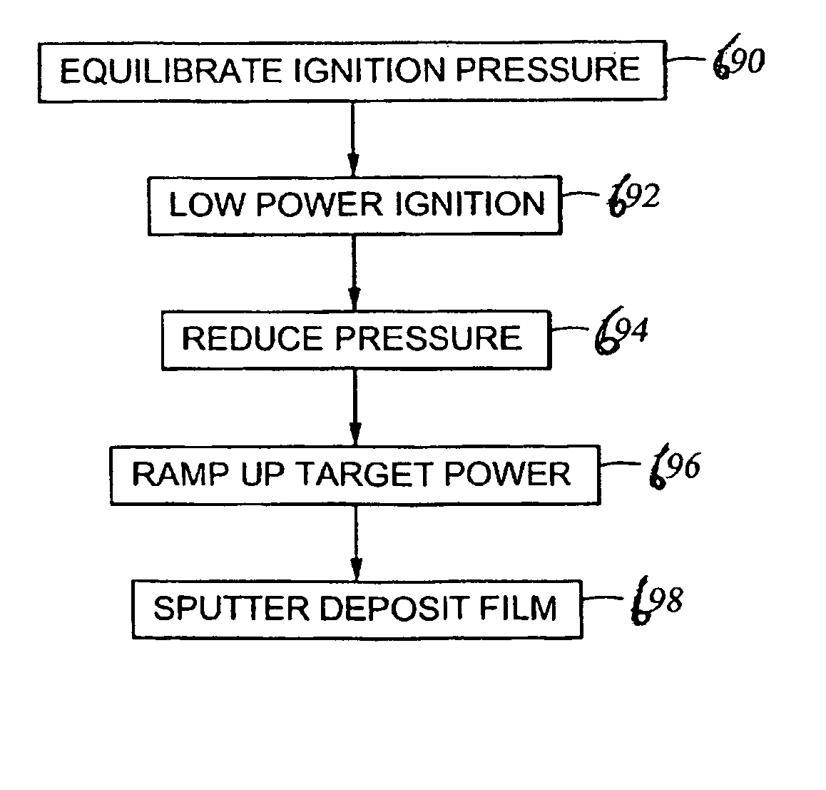
[0028] One embodiment of the present invention is directed to sputter depositing a liner material such as tantalum or tantalum nitride, by combining long-throw sputtering, self-ionized plasma (SIP) sputtering, inductively-coupled plasma (ICP) resputtering, and coil sputtering in one chamber. Long-throw sputtering is characterized by a relatively high ratio of the target-to-substrate distance and the substrate diameter. Long-throw SIP sputtering promotes deep hole coating of both the ionized and neutral deposition material components. ICP resputtering can reduce the thickness of layer bottom coverage of deep holes to reduce contact resistance. During ICP resputtering, ICP coil sputtering can deposit a protective layer, particularly on areas such as adjacent the hole openings where thinning by resputtering may not be desired.

[0029] Another embodiment of the present invention is directed to sputter depositing an interconnect material such as copper, by combining long-throw sputtering,...


PUM

PropertyMeasurementUnit
power levelaaaaaaaaaa
poweraaaaaaaaaa
poweraaaaaaaaaa

Abstract

A magnetron sputter reactor (410) and its method of use, in which SIP sputtering and ICP sputtering are promoted is disclosed. In another chamber (412) an array of auxiliary magnets positioned along sidewalls (414) of a magnetron sputter reactor on a side towards the wafer from the target is disclosed. The magnetron (436) preferably is a small one having a stronger outer pole (442) of a first polarity surrounding a weaker inner pole (440) of a second polarity all on a yoke (444) and rotates about the axis (438) of the chamber using rotation means (446, 448, 450). The auxiliary magnets (462) preferably have the first polarity to draw the unbalanced magnetic field (460) towards the wafer (424), which is on a pedestal (422) supplied with power (454). Argon (426) is supplied through a valve (428). The target (416) is supplied with power (434).

Description

RELATED APPLICATIONS [0001] This application is a continuation in part application of pending application Ser. No 09 / 685,978 filed Oct. 10, 2000, a divisional application of application Ser. No. 09 / 414,614 filed Oct. 8, 1999 (issued as U.S. Pat. No. 6,398,929); and is a continuation in part of pending application Ser. No. 10 / 202,778, filed Jul. 25, 2002 (which claims priority to provisional applications 60 / 316,137 filed Aug. 30, 2001, and 60 / 342,608 filed Dec. 21, 2001); and is a continuation in part application of pending application Ser. No. 09 / 993,543, filed Nov. 14, 2001, which are incorporated by reference in their entireties.FIELD OF THE INVENTION [0002] The invention relates generally to sputtering and resputtering. In particular, the invention relates to the sputter deposition of material and resputtering of deposited material in the formation of semiconductor integrated circuits. BACKGROUND ART [0003] Semiconductor integrated circuits typically include multiple levels of me...

Claims


Application Information

Patent Timeline
Patent Type & Authority Applications(United States)
IPC IPC(8): C23C14/04C23C14/34C23C14/35C23C14/56H01J37/32H01J37/34H01L21/285H01L21/4763H01L21/768
CPCC23C14/358C23C14/564C23C14/3457C23C14/345H01L21/76877C23C14/046H01L2221/1089H01L21/76876H01L21/76873H01L21/76871H01L21/76868H01L21/76865H01L21/76862H01L21/76846H01L21/76844H01L21/76843H01L21/76814H01L21/76805H01L21/2855H01J2237/3327H01J37/3441H01J37/3408H01J37/3402H01J37/321C23C14/568C23C14/35
Inventor DING, PEIJUNTAO, RONGXU, ZHENGLUBBEN, DANIEL C.RENGARAJAN, SURAJMILLER, MICHAEL A.SUNDARRAJAN, ARVINDTANG, XIANMINFORSTER, JOHN C.FU, JIANMINGMOSELY, RODERICK C.CHEN, FUSENGOPALRAJA, PRABURAM
Owner APPLIED MATERIALS INC
Why Eureka
Try Eureka