

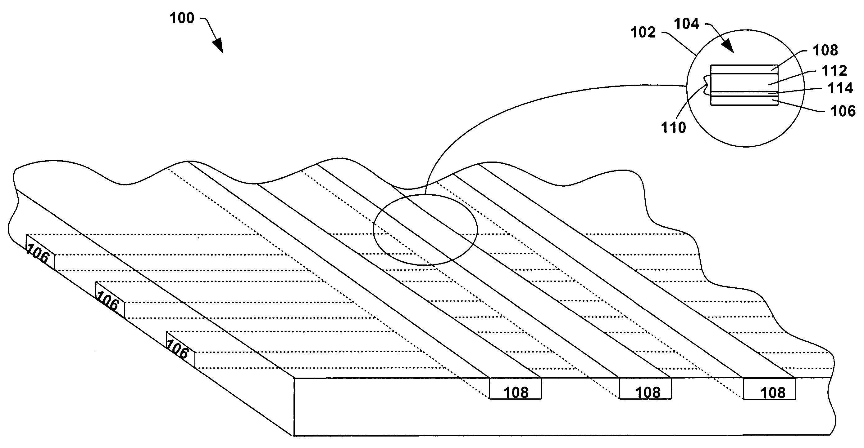
Memory device and methods of using and making the device
a memory device and memory technology, applied in thermoelectric devices, instruments, nanoinformatics, etc., can solve the problems of high cost and loss of data storage density, high electric power consumption, and the fundamental physical size limit of silicon-based devices, and achieve low operating voltage, short resistance/impedance switch time, and small size
- Summary
- Abstract
- Description
- Claims
- Application Information
AI Technical Summary
Benefits of technology
Problems solved by technology
Method used
Image

Examples
example 2
Memory cells are formed using an upper electrode of copper having a thickness of 1,000 Å and a lower electrode of copper having a thickness of 1,000 Å. A passive layer of copper sulfide having a thickness of 70 Å is provided over the lower electrode. A Cu2O as a first active layer having a thickness of 2 nm is formed over the copper sulfide using a thermal heating technique. An organic polymer layer containing polyacetylene and having a thickness of 900 Å as a second active layer is formed over the Cu2O first active layer using CVD techniques. The upper electrode is then affixed over the polymer layer.
example 3
Memory cells are formed using an upper electrode of aluminum having a thickness of 1,500 Å and a lower electrode of copper having a thickness of 1,000 Å. A passive layer of copper sulfide having a thickness of 65 Å is provided over the lower electrode. An organic semiconductor layer containing polyphenylacetylene and having a thickness of 700 Å is formed over the passive layer using CVD techniques. The upper electrode is then affixed over the polymer layer.
example 4
Memory cells are formed using an upper electrode of copper having a thickness of 1,500 Å and a lower electrode of copper having a thickness of 1,000 Å. A passive layer of copper sulfide having a thickness of 25 Å is provided over the lower electrode. An organic semiconductor layer containing polythiophene with Cu2S nanoparticles embedded therein and having a thickness of 700 Å is formed over the passive layer using spin-on and CVD techniques. The upper electrode is then affixed over the polymer layer.
PUM
| Property | Measurement | Unit |
|---|---|---|
| Thickness | aaaaa | aaaaa |
| Thickness | aaaaa | aaaaa |
| Thickness | aaaaa | aaaaa |
Abstract
Description
Claims
Application Information