Photoelectric conversion device fabrication method, photoelectric conversion device, electronic apparatus manufacturing method, electronic apparatus, metal film formation method and layer structure, and semiconductor fine particle layer and layer structure

a technology of photoelectric conversion device and fabrication method, which is applied in the direction of lighting and heating apparatus, heating types, and domestic stoves or ranges. it can solve the problems of productivity, the need for firing process is serious, and the polymer materials to be used for film electrodes cannot stand such a high temperature, so as to increase the protection function of intermediate films, improve the adhesion property, and reduce the film formation cost

Inactive Publication Date: 2005-01-27
SONY CORP
View PDF32 Cites 46 Cited by
  • Summary
  • Abstract
  • Description
  • Claims
  • Application Information

AI Technical Summary

Benefits of technology

[0063] Even if the thickness of the intermediate film is as thin as about several nm, the film can improve the adhesion property to the undercoating metal oxide film and the adhesion property of the semiconductor fine particle layer to the intermediate film. In order to heighten the protection function of the intermediate film for the metal oxide film from a strong acid, the thickness is preferably 15 nm or more, more preferably 30 m or more, and furthermore preferably 60 nm or more. The upper limit of the thickness of the intermediate film does not particularly exist, however f

Problems solved by technology

The necessity of the firing process is a serious problem to be overcome for producing a flexible solar cell.
That is, most of polymer materials to be used for the film electrode cannot stand such a high temperature.
However, these methods require an electrodeposition apparatus, a large scale press apparatus, and a large scale autoclave, respectively and thus have a problem of productivity.
However, as described above, when a platinum film is formed on the transparent electrode of a metal oxide such as ITO, owing to extremely inferior adhesion property of the platinum film, there occurs a problem that the film is easily peeled.
In order to prevent such a problem, there is a method for forming the platinum film after a film of tungsten or chromium having a good adhesion property to a transparent electrode of a metal oxide such as ITO is formed on the transparent electrode, however since the underlayer of the platinum film is a film of a different type metal, the platinum

Method used


Image

  • Photoelectric conversion device fabrication method, photoelectric conversion device, electronic apparatus manufacturing method, electronic apparatus, metal film formation method and layer structure, and semiconductor fine particle layer and layer structure
  • Photoelectric conversion device fabrication method, photoelectric conversion device, electronic apparatus manufacturing method, electronic apparatus, metal film formation method and layer structure, and semiconductor fine particle layer and layer structure
  • Photoelectric conversion device fabrication method, photoelectric conversion device, electronic apparatus manufacturing method, electronic apparatus, metal film formation method and layer structure, and semiconductor fine particle layer and layer structure

Examples


example 1

[0112] An example of a dye-sensitized wet type solar cell fabrication method will be described.

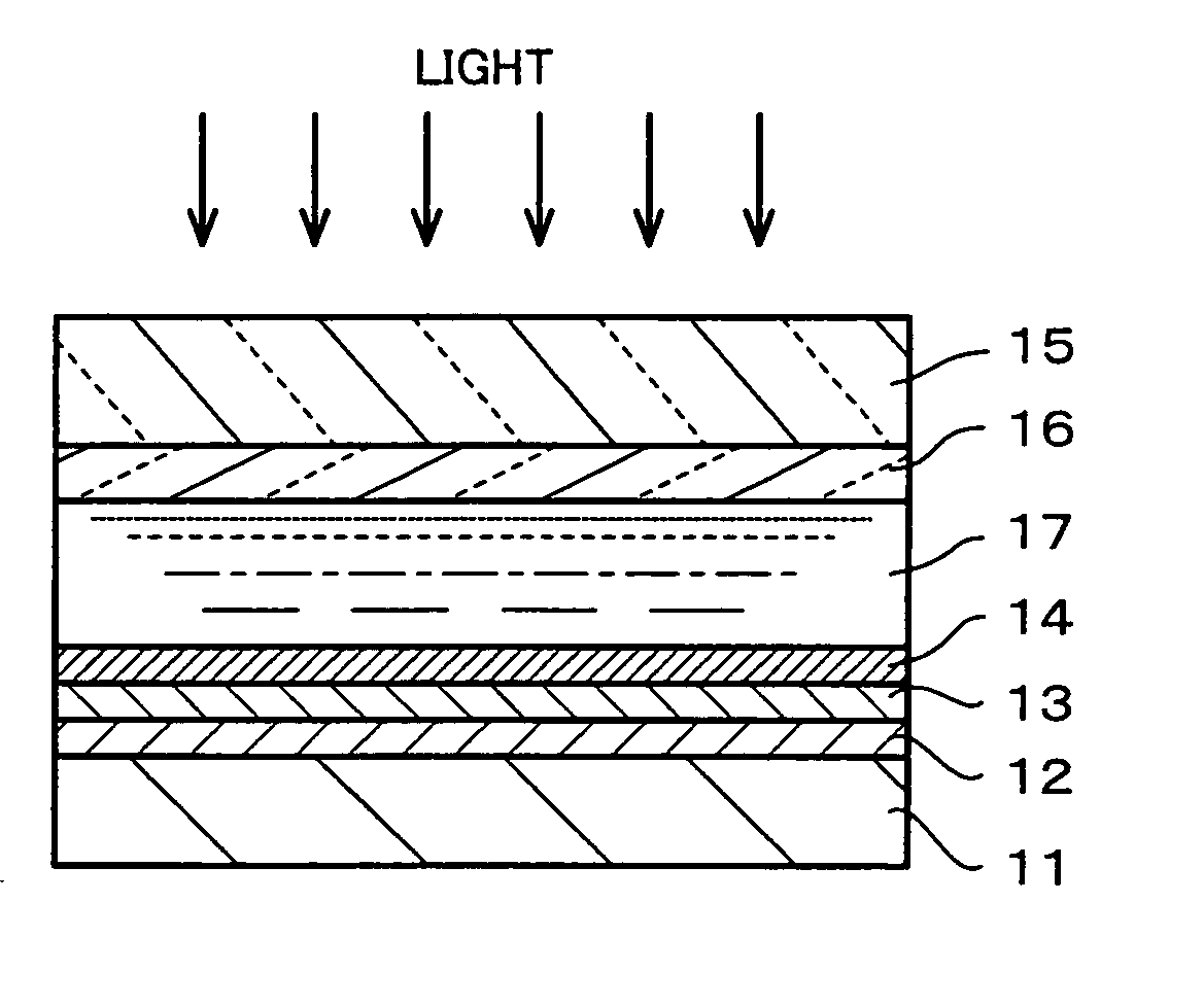
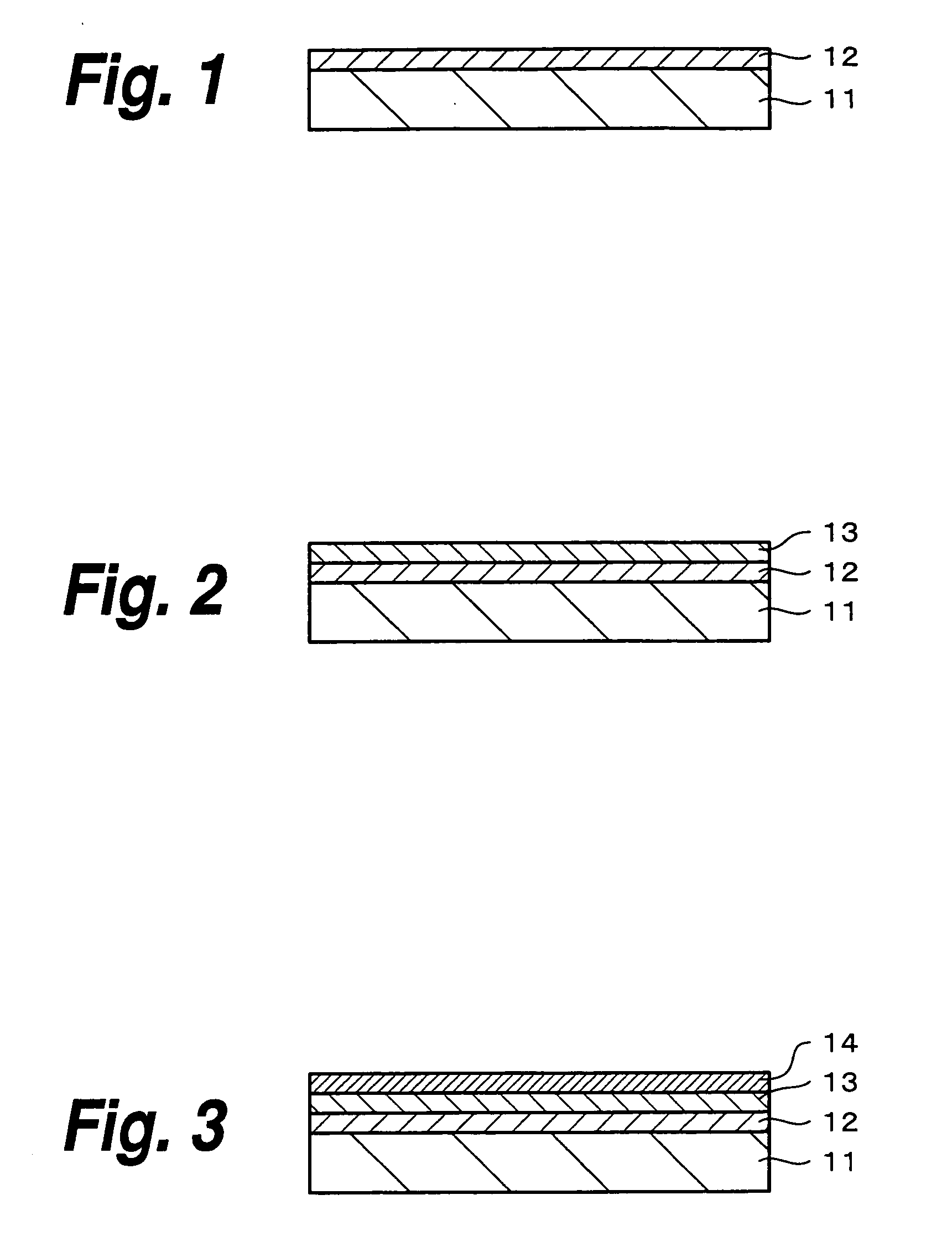
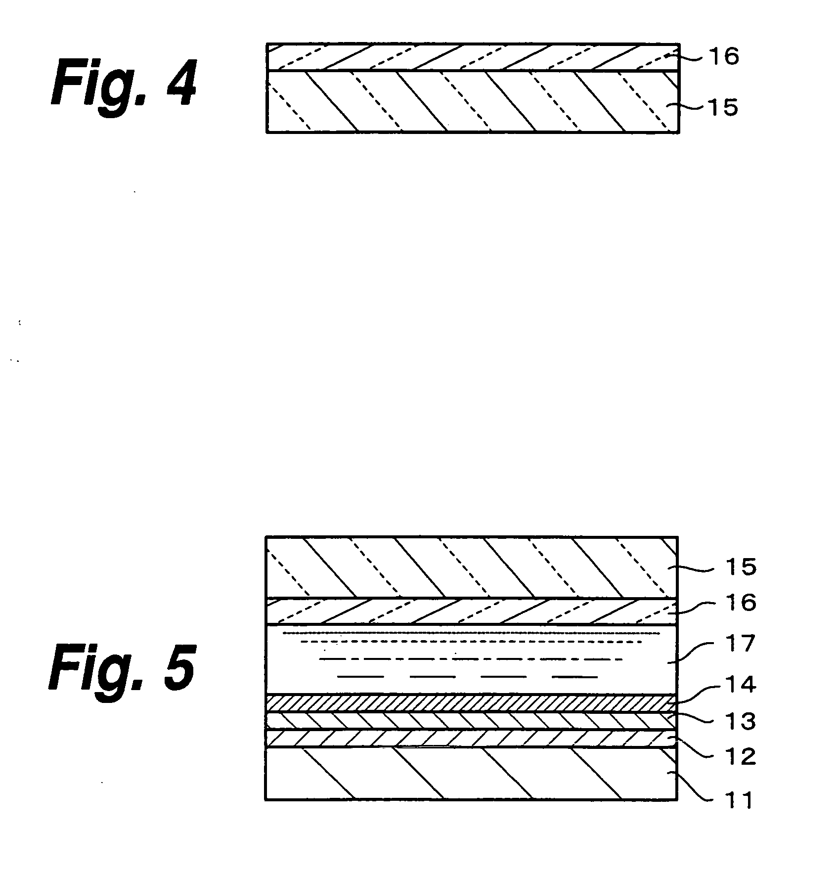
[0113] At first, as a transparent substrate 11 and transparent electrode 12, a polyethylene terephthalate (PET) film with 120 μm thickness and coated with an ITO film with a 300 nm thickness by vacuum deposition was made ready. The ITO-coated PET film was cut into 25 mm square size.

[0114] Next, the surface of the transparent electrode 12 of the ITO film was washed with pure water and then isopropanol under ultrasonic wave application for degreasing and dried in nitrogen current.

[0115] Next, an aqueous solution of 1.3 wt % of PEDOT / PSS was applied to the transparent electrode 12 of the ITO film by spin-coating at 3,000 rpm and dried on a hot plate heated to 120° C. to form a PEDOT / PSS film 13.

[0116] After that, a platinum film 14 was formed on the PEDOT / PSS film 13 by a sputtering method. The thickness of the platinum film 14 was adjusted to be 40 nm.

[0117] On the other hand, to a tita...

examples

[0133] Examples of dye-sensitized wet type solar cell fabrication methods will be described.

example 2

[0134] At first, as a transparent substrate 21 and transparent electrode 22, a polyethylene terephthalate (PET) film with 120 μm thickness and coated with an ITO film with a 300 nm thickness by vacuum deposition was made ready. The ITO-coated PET film had a sheet resistance of 10 to 30 Ω / □. The ITO-coated PET film was cut into 25 mm square size.

[0135] Next, the surface of the transparent electrode 22 of the ITO film was washed with pure water and then isopropanol under ultrasonic wave application for 15 minutes for degreasing and dried in nitrogen current.

[0136] Next, a PEDOT / PSS film 23 was formed on the transparent electrode 22, which was the ITO film, as follows. At first, the transparent substrate 21 coated with the transparent electrode 22, that is the ITO-coated PET film, was fixed on a glass substrate and being united with the glass substrate, the transparent substrate 21 was set in a spin coater. Next, an aqueous solution of 1.3 wt % of PEDOT / PSS was spread on the ITO-coat...


PUM

PropertyMeasurementUnit
Temperatureaaaaaaaaaa

Abstract

With respect to a photoelectric conversion device comprising a semiconductor electrode composed of semiconductor fine particles and a metal film to be an opposite electrode, a polyethylene dioxythiophene (PEDOT)/polystyrenesulfonic acid (PSS) film is formed by spin coating on a transparent electrode of a metal oxide such as ITO to remarkably improve the adhesion property of the metal film to the metal oxide film and the pollution by the different type metal of the metal film to be the opposite electrode can be prevented in the photoelectric conversion device. Further, a semiconductor electrode composed of semiconductor fine particles can be formed well on the metal oxide film by low temperature process while elution of the metal oxide film is prevented to obtain the photoelectric conversion device.

Description

BACKGROUND OF THE INVENTION [0001] 1. Field of the Invention [0002] The invention relates to a photoelectric conversion device fabrication method, a photoelectric conversion device, an electronic apparatus manufacturing method, an electronic apparatus, a metal film formation method and its layer structure, and a semiconductor fine particle layer and its layer structure and particularly to those suitable for application to a wet type solar cell comprising a semiconductor electrode of semiconductor fine particles. [0003] 2. Description of the Related Arts [0004] A dye-sensitized solar cell comprising a semiconductor with a high band gap sensitized by a dye is an economical solar cell of great promise in place of a conventional solar cell comprising silicon or a compound semiconductor and today it has enthusiastically been investigated (Nature, 353 (1991) 737). [0005] Investigations have been carried out so far mainly focusing on the improvement of the cell efficiency to the maximum ex...

Claims


Application Information

Patent Timeline
IPC IPC(8): H01G9/20H01L31/02H01L51/00H01L51/30H01L51/42
CPCH01G9/2022Y02E10/542H01L51/0037H01G9/2031H10K85/1135A47J37/0629F24C7/04F24C15/14
Inventor ENOMOTO, MASASHIHONDA, TOSHIO
Owner SONY CORP
Why Eureka
Try Eureka