
Method of manufacturing a semiconductor integrated circuit device

a semiconductor and integrated circuit technology, applied in the direction of semiconductor devices, electrical equipment, transistors, etc., can solve the problems of reducing the carrier mobility of misfet, the dielectric constant of silicon oxynitride films is difficult to increase, and the drain current (ids) is about 10%

Inactive Publication Date: 2005-01-27
RENESAS ELECTRONICS CORP
View PDF9 Cites 2 Cited by
  • Summary
  • Abstract
  • Description
  • Claims
  • Application Information

AI Technical Summary

Benefits of technology

[0012] However, it is difficult to increase the dielectric constant of the silicon oxynitride film, formed by the conventional oxynitridation treatment in which nitrogen is introduced into a silicon nitride film by heating a substrate in a NO gas or N2O gas atmosphere, by increasing the concentration of nitrogen contained in the entire film because the surface of the film is not nitrided although the concentration of nitrogen near the interface between the film and the substrate can be increased.
[0014]FIG. 30 is a graph showing the relationship between the concentration of nitrogen at the interface between the gate insulating film and the substrate and the carrier mobility of MISFET. As shown in the graph, in the case of an n channel MISFET in which electrons are carriers, when several atomic percents of nitrogen is introduced into the interface, the carrier mobility becomes higher than when nitrogen is not introduced but when the concentration of nitrogen further increases, the above effect gradually decreases. Meanwhile, in the case of a p channel MISFET in which electron holes are carriers, the carrier mobility becomes lower in proportion to the concentration of nitrogen at the interface. When the concentration of nitrogen is higher than 10 atomic %, the carrier mobility drops by about 20%, thereby reducing the drain current (Ids) by about 10% and making difficult circuit design practically.
[0018] It is another object of the present invention to provide a technology capable of improving the reliability of a semiconductor integrated circuit device comprising a silicon oxynitride film as a gate insulating film for MISFET.
[0026] According to the above means, since a gate insulating film can be formed from silicon oxynitride by using both an oxynitridation treatment and a nitrogen plasma treatment, the concentration of nitrogen contained in the gate insulating film can be increased without raising the concentration of nitrogen near the interface between the substrate and the gate insulating film to a higher level than required.

Problems solved by technology

However, it is difficult to increase the dielectric constant of the silicon oxynitride film, formed by the conventional oxynitridation treatment in which nitrogen is introduced into a silicon nitride film by heating a substrate in a NO gas or N2O gas atmosphere, by increasing the concentration of nitrogen contained in the entire film because the surface of the film is not nitrided although the concentration of nitrogen near the interface between the film and the substrate can be increased.
When a portion near the interface between the gate insulating film and the substrate is nitrided excessively, a trap in the interfacial level or the film increases, thereby causing a problem such as a reduction in the carrier mobility of MISFET.
When the concentration of nitrogen is higher than 10 atomic %, the carrier mobility drops by about 20%, thereby reducing the drain current (Ids) by about 10% and making difficult circuit design practically.

Method used


Image

  • Method of manufacturing a semiconductor integrated circuit device
  • Method of manufacturing a semiconductor integrated circuit device
  • Method of manufacturing a semiconductor integrated circuit device

Examples


embodiment 1

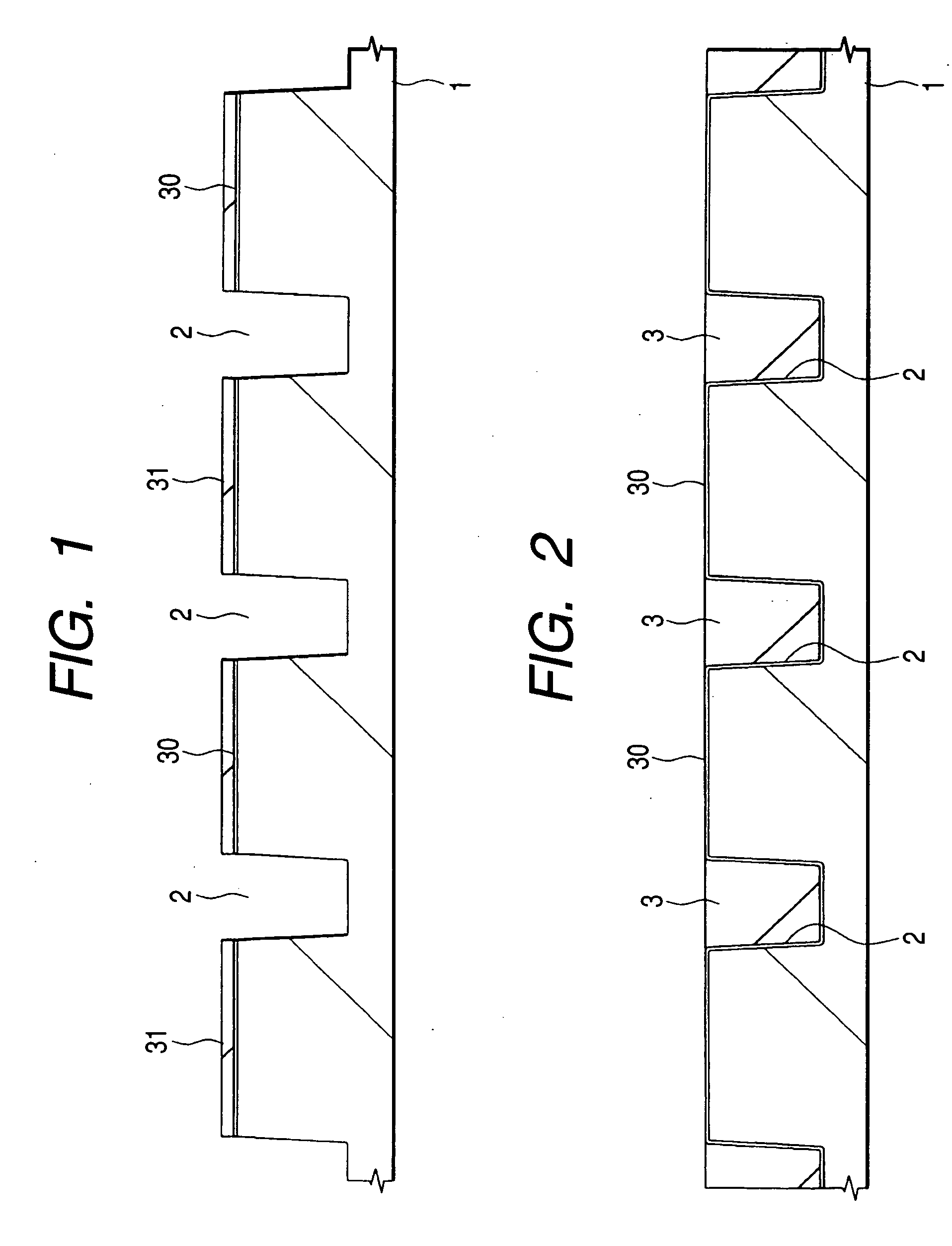
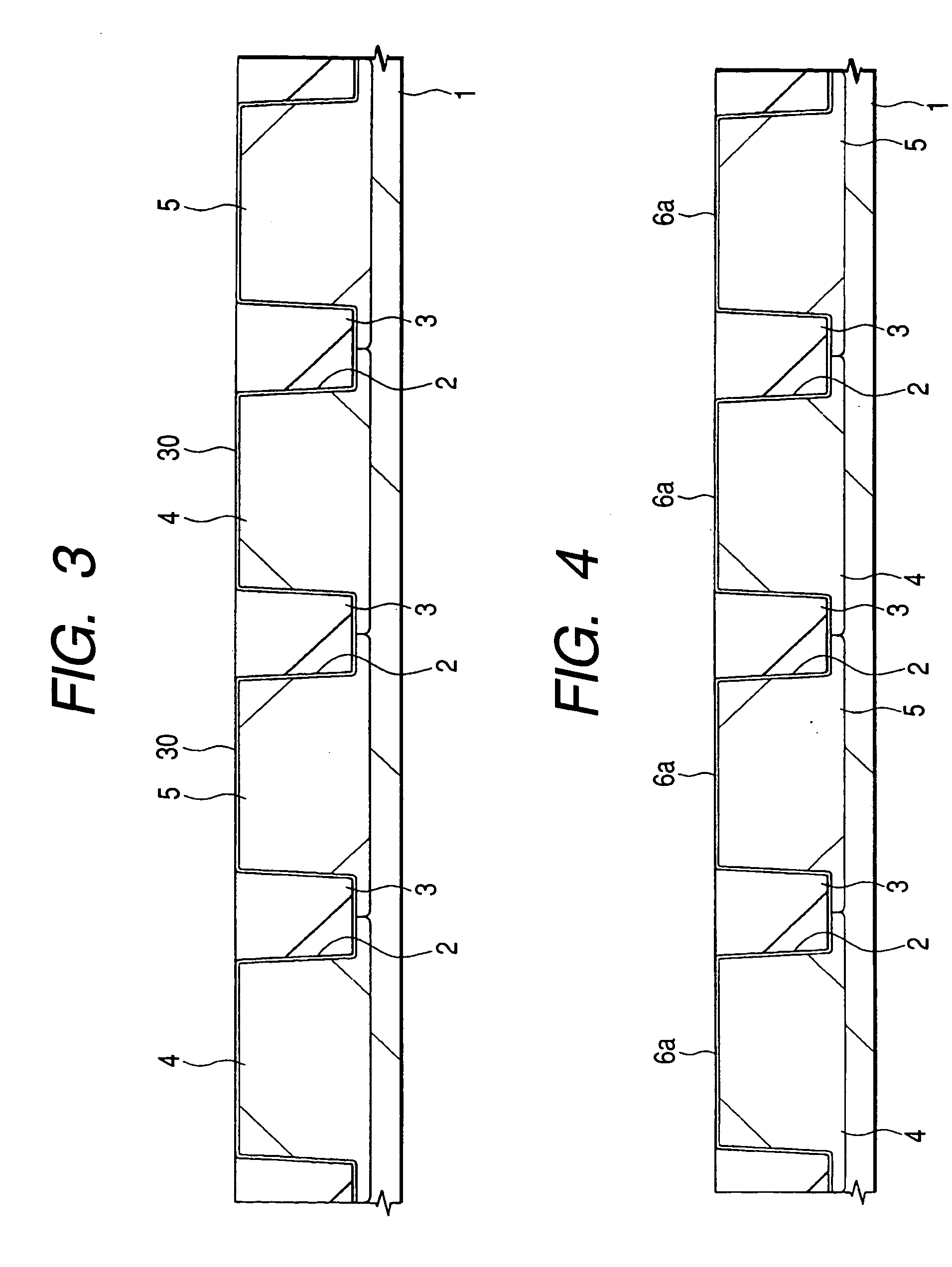
[0066] The method of manufacturing a CMOS-LSI according to this embodiment will be described in the order of steps with reference to FIGS. 1 to 15.

[0067] First, as shown in FIG. 1, element separation grooves 2 are formed in the main surface of a semiconductor substrate (to be referred to as “substrate” hereinafter) made from p type monocrystal silicon having a resistivity of about 1 to 10 Ωcm. To form the element separation grooves 2, the substrate 1 is thermally oxidized to form a silicon oxide film 30 having a thickness of about 10 nm on the surface, a silicon nitride film 31 having a thickness of about 100 nm deposited on the top of the silicon oxide film 30 by CVD is patterned, and then the substrate 1 is etched by using this silicon nitride film 31 as a mask.

[0068] Thereafter, as shown in FIG. 2, a silicon oxide film 3 having a thickness of about 500 nm is deposited on the substrate 1 by CVD, the silicon oxide film 3 around the element separation grooves 2 is removed by a che...

embodiment 2

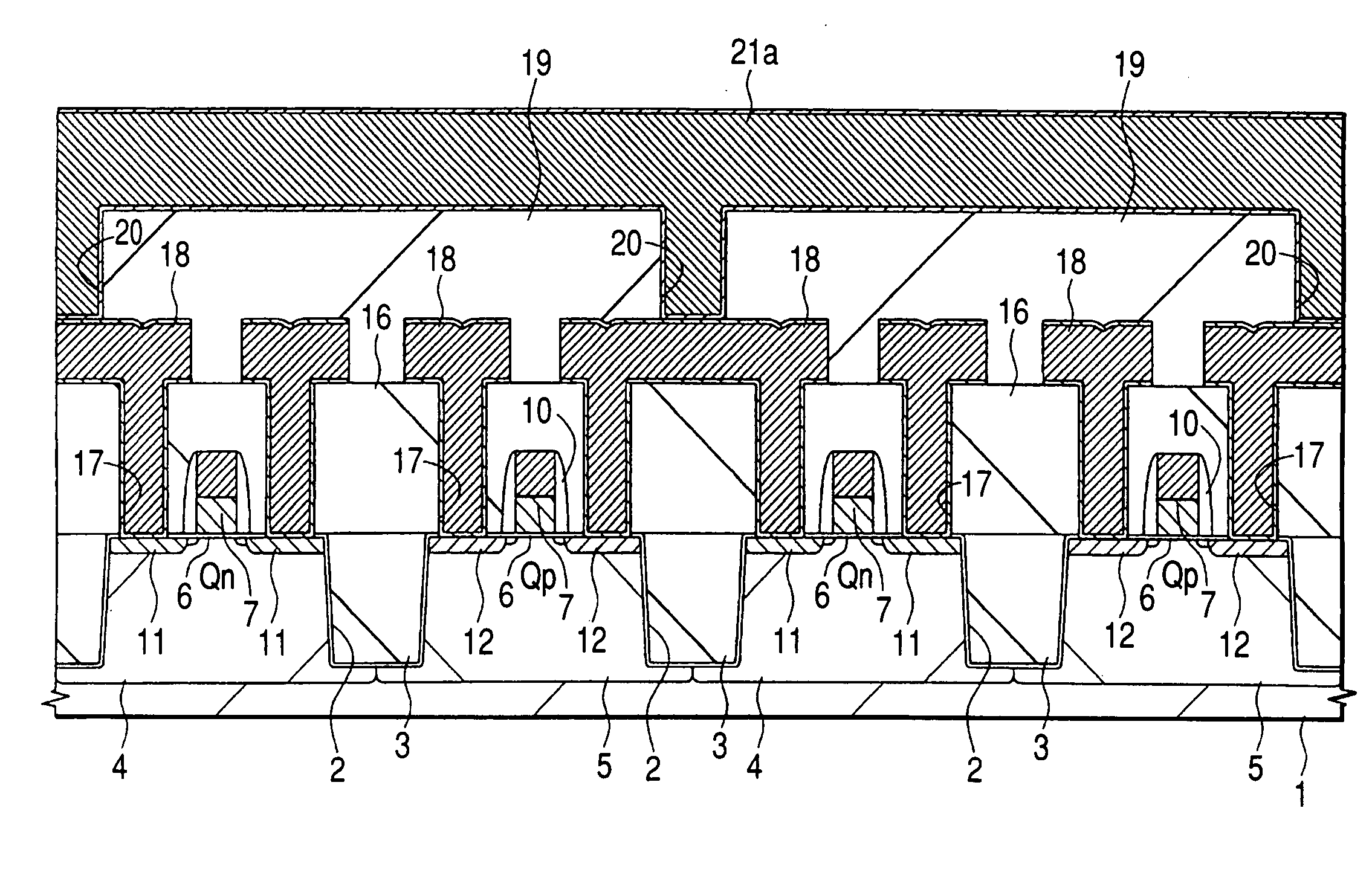
[0094] The semiconductor integrated circuit device of this embodiment is a DRAM-logic hybrid LSI having a DRAM (Dynamic Random Access Memory) and a logic circuit formed on the same semiconductor substrate. The method of manufacturing this hybrid LSI will be described in the order of steps with reference to FIGS. 16 to 26. The left and center areas in these figures are a DRAM memory cell forming area (to be referred to as “DRAM forming area” hereinafter) and the right area is a logic circuit forming area.

[0095] As shown in FIG. 16, element separation grooves 2, p type wells 4 and an n type well 5 are first formed on the main surface of a substrate 1 in the same manner as in the above Embodiment 1, a silicon oxide film 6a is formed on the surfaces of the p type wells 4 and the n type well 5, nitrogen is introduced into the silicon oxide film 6a by using both of the above oxynitridation treatment and nitrogen plasma treatment to form a silicon oxynitride gate insulating film 6 having ...

embodiment 3

[0114] The method of forming a gate insulating film according to this embodiment will be described with reference to FIGS. 27 to 29.

[0115] As shown in FIG. 27, element separation grooves 2 , p type wells 4 and n type wells 5 are formed on the main surface of the substrate 1, and the substrate 1 is wet oxidized to form a silicon oxide film 6a having a thickness of 1 to 1.5 nm on the surfaces of the p type wells 4 and the n type wells 5 in the same manner as in the above Embodiment 1.

[0116] As shown in FIG. 28, the substrate 1 is heated in an atmosphere containing 5% of an NO gas at 900 to 1,100° C. Thereby, nitrogen is introduced into the silicon oxide film 6a formed on the surface of the substrate 1 and a silicon oxynitride film 6b in which nitrogen segregates near the interface with the substrate 1 is formed as in the above Embodiment 1. Conditions for carrying out the above heat treatment (oxynitridation treatment) must be set to ensure that the concentration of nitrogen near th...


PUM

PropertyMeasurementUnit
thicknessaaaaaaaaaa
temperatureaaaaaaaaaa
thicknessaaaaaaaaaa

Abstract

A method of manufacturing a semiconductor integrated circuit device comprising forming a silicon oxide film as thin as 5 nm or less on the surfaces of p type wells and n type wells by wet oxidizing a substrate, heating the substrate in an atmosphere containing about 5% of an NO gas to introduce nitrogen into the silicon oxide film so as to form a silicon oxynitride film, exposing the substrate to a nitrogen plasma atmosphere to further introduce nitrogen into the silicon oxynitride film in order to form a silicon oxynitride gate insulating film having a first peak concentration near the interface with the substrate and a second peak concentration near the surface thereof. Thereby, the concentration of nitrogen in the gate insulating film is increased without raising the concentration of nitrogen near the interface between the substrate and the gate insulating film to a higher level than required.

Description

BACKGROUND OF THE INVENTION [0001] The present invention relates to a semiconductor integrated circuit device and to a manufacture technology for the same and, specifically, to a technology which is effectively applied to a semiconductor integrated circuit device comprising a silicon oxynitride film as a gate insulating film for MISFET (Metal Insulator Semiconductor Field Effect Transistor). [0002] To realize the low-voltage operation of MISFET, a gate oxide film must be made thinner in proportion to a reduction in the thickness of MISFET. However, when the thickness of the gate oxide film is reduced, a direct tunnel current running through the film grows, thereby causing a gate leak current which cannot be ignored from the viewpoint of reducing power consumption. [0003] To cope with this, attempts have been made to increase the physical thickness of the gate insulating film by using a high dielectric film such as a titanium oxide (TiO2) or tantalum oxide (Ta2O5) film having a highe...

Claims


Application Information

Patent Timeline
Patent Type & Authority Applications(United States)
IPC IPC(8): H01L27/04H01L21/28H01L21/314H01L21/822H01L21/8234H01L21/8238H01L21/8242H01L27/092H01L27/10H01L27/108H01L29/51H01L29/78
CPCH01L21/28185H01L27/1052H01L21/3143H01L21/82345H01L21/823462H01L21/823842H01L21/823857H01L27/10814H01L27/10888H01L27/10894H01L29/513H01L29/518H01L29/6659H01L29/7833H01L21/28202H01L21/0214H10B12/315H10B12/485H10B12/09H01L29/78H01L21/02332H10B99/00
Inventor ISHIKAWA, DAISAKAI, SATOSHIHIRAIWA, ATSUSHI
Owner RENESAS ELECTRONICS CORP
Learn More