

Method and apparatus for producing photocatalyst
a photocatalyst and photocatalyst technology, applied in the direction of catalyst activation/preparation, physical/chemical process catalysts, metal/metal-oxide/metal-hydroxide catalysts, etc., can solve the problems of photocatalysis tending to be deteriorated, imposing considerable limitations on available substrates in terms of heat resistance, and poor durability of photocatalytic films
- Summary
- Abstract
- Description
- Claims
- Application Information
AI Technical Summary
Benefits of technology
Problems solved by technology
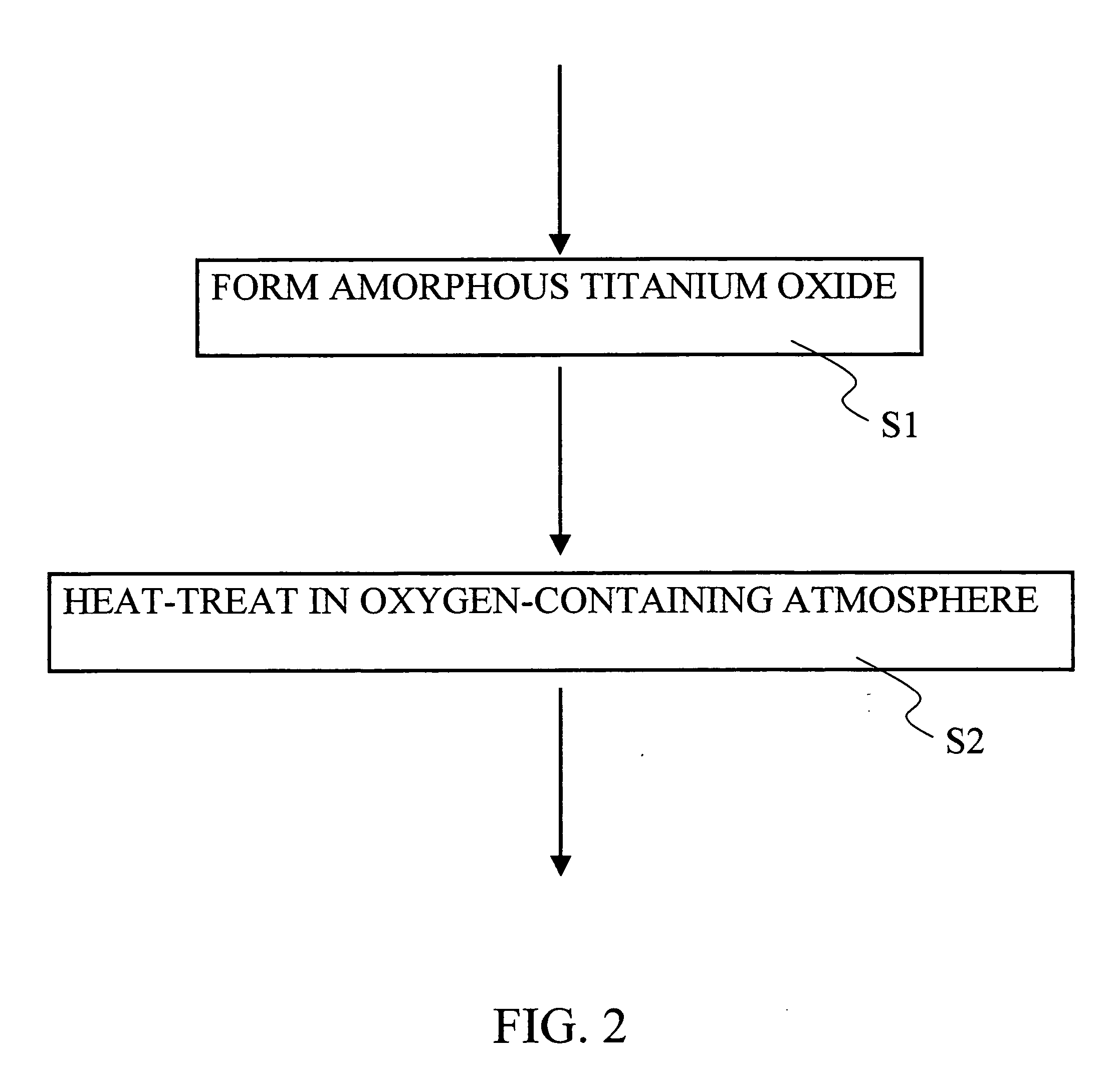
Method used
Image

Examples
first embodiment
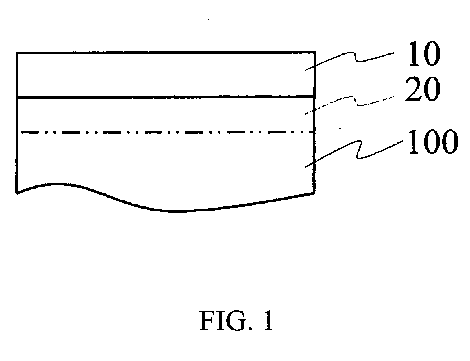
[0055]FIG. 1 is a schematic view illustrating a cross-sectional structure of a photocatalyst produced in accordance with the invention.
[0056] The photocatalyst comprises a photocatalytic film 10 formed in a thin film on a substrate 100. The substrate 100 may be made of various materials such as inorganic materials including glass and ceramics, metallic materials including stainless steel, or organic materials including polymer materials, and may have various shapes and sizes.
[0057] The photocatalytic film 10 may be made of a semiconductor material primarily composed of metal oxides. The semiconductor may include, for example, titaniumoxide (TiOx), zinc oxide (ZnOx), tin oxide (SnOx) or other metal oxides. Among others, titanium oxide is active as a photocatalyst, and superior in stability, safety and other respects. Accordingly, an example will hereinafter be described where titanium oxide is used as a metal oxide.
[0058] A buffer layer 20 may be formed between the photocatalytic f...
second embodiment
[0128] Now, as the invention, a method of producing a photocatalyst having a coating layer of silicon oxide or the like on a photocatalytic film will be described.
[0129]FIG. 16 is a schematic diagram illustrating a cross-sectional structure of a photocatalyst produced in accordance with a second embodiment of the invention.
[0130] More specifically, the photocatalyst in accordance with the present embodiment comprises, as with that described above with reference to FIG. 1, a photocatalytic film 10 on a substrate 100 with a buffer layer 20 of silicon oxide or the like being interposed as appropriate in between. Since the substrate 100, buffer layer 20, and photocatalytic film 10 can be the same as those described above with reference to the first embodiment, they are labeled with like reference numerals and will not be described further in detail.
[0131] In the present embodiment, a coating layer 30 is further provided on the photocatalytic film 10.
[0132] The coating layer 30 serves...
PUM
| Property | Measurement | Unit |
|---|---|---|
| partial pressure | aaaaa | aaaaa |
| partial pressure | aaaaa | aaaaa |
| temperature | aaaaa | aaaaa |
Abstract
Description
Claims
Application Information