Si/SiGe optoelectronic integrated circuits
Inactive Publication Date: 2005-02-03
GLOBALFOUNDRIES INC
11 Cites 35 Cited by
AI-Extracted Technical Summary
Problems solved by technology
However, the intrinsic material properties of Si are much less favorable compared to GaAs.
Therefore, for a Si photodetector to have high responsivity it must have a thick absorbing region making the detector very slow, and for high speed the absorbing region should be very thin resulting in an extremely poor responsivity.
However such a technique is limited to use with SOI substrates, and may not be suitable for practical applications due to the complexities of the roughening process.
Si photodetectors are further hindered by the fact that the electron mobility in Si/...
Method used
[0035] In one embodiment, the subsequent layers are a Si quantum well layer 4, a Si1-yGey undoped or not-intentionally doped offset layer 5, a doped Si1-yGey supply layer 6 and optionally a Si layer 7. By an undoped layer, it is meant a not-intentionally doped layer which may have a background dopant concentration so low as to not substantially affect the function of the layer. The Ge composition of layers 5 and 6 are in the range of y=0.1 to 1.0 and y is preferably the same as the composition of layer 3. A quantum well for electrons is formed in Si layer 4 due to the conduction band splitting arising from the tensile strain in Si layer 4. The isolation for MODFET 15 is achieved by forming an etched mesa region, thereby exposing the surface 8 of Si1-yGey buffer layer 3 in the etched regions, as shown in FIG. 1B. Next, in FIG. 1C, n-type implanted regions 9 are formed to facilitate making low-resistance contacts to the Si quantum well layer 4. The source and drain metallization 10 can then be deposited as depicted in FIG. 1D, followed by the gate metallization 12 shown in FIG. 1E.
[0036] The MSM photodetector is created by depositing interdigitated Schottky electrodes 11 on the exposed surface 8 of buffer layer 3. To simplify the fabrication process, it is possible for MSM electrodes 11 to be defined in the same lithographic step as the Ohmic metallization 10, as depicted in FIG. 1D. MSM electrodes 11 are configured in such a way such that a bias applied between adjacent electrodes, as shown in FIG. 1E, creates an electric field that penetrates into the underlying absorbing layer 3. Light or radiant 14 energy incident from or passing through surface 8 creates free carriers, electrons 15 and holes 16, in layer 3 that travel to electrodes 11, creating a current signal that is proportional to the power of the incident light.
[0038]FIG. 3 shows another embodiment of the invention that is the same as that shown in FIG. 1E, except that the MSM photodetector is surrounded by a deep isolation trench 23 that extends from the surface 8 of the relaxed buffer layer 3 down into the substrate 1. Isolation trench 23 serves to confine the carriers that are generated in Si1-yGey buffer layer 3 from diffusing laterally outside the region directly beneath the detector geometry. The trench also serves to isolate slow carriers generated outside the high-field region directly beneath the detector geometry from being collected by the surface electrodes 11, thereby leading to improved high-frequency performance. Furthermore, deep isolation trench 23 can be planarized by filling with a dielectric material 24. The trench can readily be incorporated into the fabrication scheme shown in FIGS. 1A-1E, by etching deep isolation trench 23 before the mesa isolation in FIG. 1B, then filling the trench with dielectric material 24, followed by a planarization step. The subsequent fabrication steps can then be performed as depicted in FIG. 1B-1E.
[0039]FIG. 4A shows another embodiment of the invention that is the same as that shown in FIG. 1E, except that the relaxed buffer layer 38, over layer 2, is composed of a symmetrically strained superlattice instead of a constant-composition alloy Si1-yGey. The superlattice consists of alternating layers of Si1-xGex, 35, and Si1-zGez, 36, where x38 is equal to y where y is in the range from 0.1 to 0.9, with a preferred value of 0.25. The tensile strain in Si1-xGex layer 35, and the compressive strain in Si1-zGez layer 36 enhances the absorption of radiation by reducing the effective band gap of buffer layer 38. To ensure that the photogenerated carriers are not trapped in the potential wells formed by strained layers 35 and 36, the Ge composition of buffer layer 38 can be graded in a continuous fashion, to produce a smooth, rather than abrupt, potential profile. This situation is shown schematically in FIG. 4B, where the conduction and valence band edges, shown by curves 41 and 42, of alternating strained layers 35 and 36 are plotted along with the conduction and valence band edges, shown by curves 43 and 44, of a constant composition layer. The average band gap of the symmetric superlattice Eg2, shown by arrow 45, is reduced compared to that of the constant composition layer, Eg1, shown by arrow 46, leading to greater photoabsorption in the symmetric superlattice. The operation of the MODFET 15 structure shown in FIG. 4A is not affected by the symmetric superlattice because no net strain is built up in layer 38. Therefore, after the growth of the superlattice 38, only a thin, constant-composition Si1-yGey layer 37, needs to be deposited before growing the MODFET 15 layers 4-7. For layer 37, y is in the range from 0.1 to 0.9, and is preferably equal to the average Ge-composition of layer 38.
[0041] As the Ge content of the buffer layers is increased, the band gap shrinks, leading to larger dark currents for the photodiode. A method of reducing the dark current without a dramatic increase in process com...
Benefits of technology
[0014] A design and method of fabricating an optoelectronic integrated circuit (OEIC) on a Si substrate is presented. This is achieved by using a high-quality, Si/SiGe heterostructure grown on a Si substrate to monolithically integrate a high-speed and responsivity SiGe photodetector and a modulation-doped field effect transistor on the same wafer. A typical layer structure consists of a Si substrate, a graded Ge-content Si1-xGex buffer layer, a thick, undoped relaxed Si1-yGey buffer layer, a Si quantum well, a Si1-yGey undoped offset layer, a doped Si1-yGey supply layer, and optionally a Si surface layer may be incorporated. A MODFET can be fabricated on the layer structure using mesa isolation, and by defining source, drain and gate electrod...
Abstract
An integrated optoelectronic circuit and process for making is described incorporating a photodetector and a MODFET on a chip. The chip contains a single-crystal semiconductor substrate, a buffer layer of SiGe graded in composition, a relaxed SiGe layer, a quantum well layer, an undoped SiGe spacer layer and a doped SiGe supply layer. The photodetector may be a metal-semiconductor-metal (MSM) or a p-i-n device. The detector may be integrated with an n- or p-type MODFET, or both in a CMOS configuration, and the MODFET can incorporate a Schottky or insulating gate. The invention overcomes the problem of producing Si-manufacturing-compatible monolithic high-speed optoelectronic circuits for 850 nm operation by using epixially-grown Si/SiGe heterostructure layers.
Application Domain
Solid-state devicesSemiconductor/solid-state device manufacturing +3
Technology Topic
PhotodetectorCMOS +5
Image
Examples
- Experimental program(1)
Example
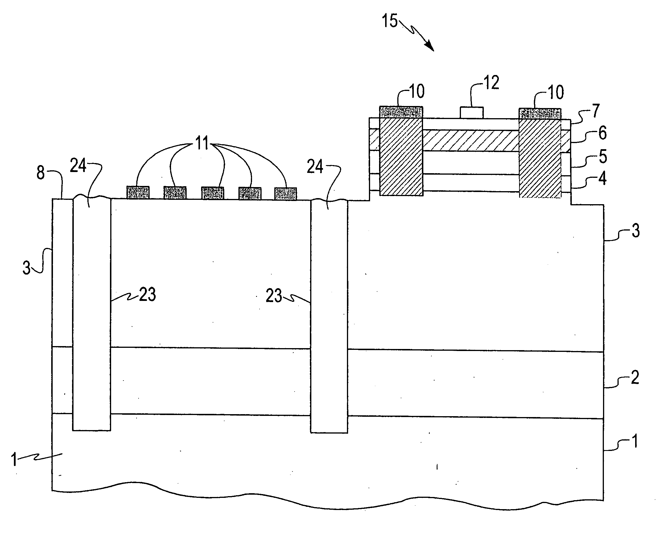
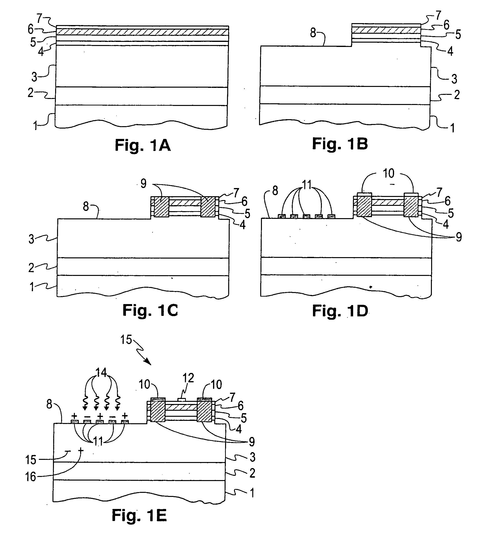
[0034]FIGS. 1A-1E show the fabrication sequence for one embodiment of the invention where an n-channel, Si/SiGe modulation-doped field effect transistor (MODFET) 15 is integrated with a SiGe metal-semiconductor-metal (SM) photodetector. A typical layer structure is shown in FIG. 1A. The layers are epitaxially grown on a Si substrate 1 using a high-precision epitaxy technique such as molecular beam epitaxy, rapid thermal cheimcal vapor deposition, or ultra high vacuum chemical vapor deposition (UHV-CVD). Substrate 1 may also be SiGe, Ge, GaAs, SiC, SOS and SOI. Suitable adjustments will be required to accomodate a different substrate lattice constant compared to Si. The following description is directed to a Si substrate. For a description of how to grow epitaxial Si and Si1-xGex layers by UHV-CVD, reference is made to U.S. Pat. No. 5,298,452 which was issued on Mar. 29, 1994 to B. S. Meyerson which is incorporated herein by reference. For Si1-xGex layers, GeH4 is added to Si-containing gas such as SiH4 or Si2H6 in the UHV-CVD reactor. Ge is incorporated into the crystal lattice in place of Si during formation of the layer in the amount or proportion of x. Layer 2 comprises a Si1-xGex buffer layer that has a thickness in the range from 0.2 to 1.5 μm, with a preferred value of about 0.5 μm, and has a percent Ge composition that is increased from x=0 (in a continuous or stepwise fashion) to a value in the range from x=0.10 to 1.0 with a preferred value of x=0.25. Layer 2 serves to relax the strain caused by the lattice mismatch between layer 2 of graded Ge composition Si1-xGex and Si substrate 1. Ge has a lattice spacing of 1.04 times the lattice spacing of Si. Thus for a relaxed top surface of buffer layer 2 where x equals 0.25, the lattice spacing of the unit cell along each axis in the top surface is about 1.01 times the lattice spacing of the unit cell of Si along each axis. For a description of how to grow relaxed low defect top surfaces of Si1-xGex layers, reference is made to U.S. Pat. No. 5,659,187 which was issued on Aug. 19, 1997 to F. K. Legoues and B. S. Meyerson which is incorporated herein by reference. After the graded region of layer 2, a 0.25 to about 10 μm thick, undoped or not-intentionally doped layer 3 of Si1-yGey is grown, where the Ge composition, typically y=0.25, is in the range from y=0.10 to 1.0. Layer 3 acts as the absorbing medium for radiant energy as well as a relaxed, device quality pseudosubstrate for growth of subsequent layers. The background impurities in layer 3 should be low enough to allow penetration of the electric field from the surface electrodes into the entire layer.
[0035] In one embodiment, the subsequent layers are a Si quantum well layer 4, a Si1-yGey undoped or not-intentionally doped offset layer 5, a doped Si1-yGey supply layer 6 and optionally a Si layer 7. By an undoped layer, it is meant a not-intentionally doped layer which may have a background dopant concentration so low as to not substantially affect the function of the layer. The Ge composition of layers 5 and 6 are in the range of y=0.1 to 1.0 and y is preferably the same as the composition of layer 3. A quantum well for electrons is formed in Si layer 4 due to the conduction band splitting arising from the tensile strain in Si layer 4. The isolation for MODFET 15 is achieved by forming an etched mesa region, thereby exposing the surface 8 of Si1-yGey buffer layer 3 in the etched regions, as shown in FIG. 1B. Next, in FIG. 1C, n-type implanted regions 9 are formed to facilitate making low-resistance contacts to the Si quantum well layer 4. The source and drain metallization 10 can then be deposited as depicted in FIG. 1D, followed by the gate metallization 12 shown in FIG. 1E.
[0036] The MSM photodetector is created by depositing interdigitated Schottky electrodes 11 on the exposed surface 8 of buffer layer 3. To simplify the fabrication process, it is possible for MSM electrodes 11 to be defined in the same lithographic step as the Ohmic metallization 10, as depicted in FIG. 1D. MSM electrodes 11 are configured in such a way such that a bias applied between adjacent electrodes, as shown in FIG. 1E, creates an electric field that penetrates into the underlying absorbing layer 3. Light or radiant 14 energy incident from or passing through surface 8 creates free carriers, electrons 15 and holes 16, in layer 3 that travel to electrodes 11, creating a current signal that is proportional to the power of the incident light.
[0037]FIG. 2 depicts the manner in which the devices shown in FIG. 1 are connected to form a simple photoreceiver circuit 17. A bias voltage, Vdiode, is applied to the positive MSM electrode, while the negative electrode is connected to the gate of depletion-mode transistor 18, and to a bias resistor 19, Rbias, which is connected to a negative supply voltage, −Vss. The transistor source is connected to ground, while the drain is connected to a load resistor 20, Rload, which is connected to the supply voltage, Vdd. In this configuration, the photocurrent induced by the incident light creates a voltage across the bias resistor 19 which is input to the gate of the transistor 18, thereby modulating the transistor current, and creating an amplified signal at the output lead 21, Vout. Resistors 19 and 20 may be formed and interconnected on the chip with the photodetector 22 and transistor 18 which is well known in the art. Other optoelectronic circuits may be formed which for example use more transistors to optimize the circuit to the application.
[0038]FIG. 3 shows another embodiment of the invention that is the same as that shown in FIG. 1E, except that the MSM photodetector is surrounded by a deep isolation trench 23 that extends from the surface 8 of the relaxed buffer layer 3 down into the substrate 1. Isolation trench 23 serves to confine the carriers that are generated in Si1-yGey buffer layer 3 from diffusing laterally outside the region directly beneath the detector geometry. The trench also serves to isolate slow carriers generated outside the high-field region directly beneath the detector geometry from being collected by the surface electrodes 11, thereby leading to improved high-frequency performance. Furthermore, deep isolation trench 23 can be planarized by filling with a dielectric material 24. The trench can readily be incorporated into the fabrication scheme shown in FIGS. 1A-1E, by etching deep isolation trench 23 before the mesa isolation in FIG. 1B, then filling the trench with dielectric material 24, followed by a planarization step. The subsequent fabrication steps can then be performed as depicted in FIG. 1B-1E.
[0039]FIG. 4A shows another embodiment of the invention that is the same as that shown in FIG. 1E, except that the relaxed buffer layer 38, over layer 2, is composed of a symmetrically strained superlattice instead of a constant-composition alloy Si1-yGey. The superlattice consists of alternating layers of Si1-xGex, 35, and Si1-zGez, 36, where x 38 is equal to y where y is in the range from 0.1 to 0.9, with a preferred value of 0.25. The tensile strain in Si1-xGex layer 35, and the compressive strain in Si1-zGez layer 36 enhances the absorption of radiation by reducing the effective band gap of buffer layer 38. To ensure that the photogenerated carriers are not trapped in the potential wells formed by strained layers 35 and 36, the Ge composition of buffer layer 38 can be graded in a continuous fashion, to produce a smooth, rather than abrupt, potential profile. This situation is shown schematically in FIG. 4B, where the conduction and valence band edges, shown by curves 41 and 42, of alternating strained layers 35 and 36 are plotted along with the conduction and valence band edges, shown by curves 43 and 44, of a constant composition layer. The average band gap of the symmetric superlattice Eg2, shown by arrow 45, is reduced compared to that of the constant composition layer, Eg1, shown by arrow 46, leading to greater photoabsorption in the symmetric superlattice. The operation of the MODFET 15 structure shown in FIG. 4A is not affected by the symmetric superlattice because no net strain is built up in layer 38. Therefore, after the growth of the superlattice 38, only a thin, constant-composition Si1-yGey layer 37, needs to be deposited before growing the MODFET 15 layers 4-7. For layer 37, y is in the range from 0.1 to 0.9, and is preferably equal to the average Ge-composition of layer 38.
[0040] Another embodiment of the invention is shown in FIG. 5, where a SiGe MSM photodetector is integrated with a p-channel MODFET 47. This configuration consists of a graded buffer layer 2 followed by a constant composition Si1-yGey absorbing layer 3, similar to that of FIGS. 1A-1E. These layers are followed by a layer structure for a p-channel MODFET 47, consisting of a Si1-wGew, doped layer 48, where w 1-yGey layer 49, a compressive-strained Si1-zGez quantum well layer 50, where z>y, an undoped Si1-yGey layer 51, and optionally a thin Si layer 52. The Ge percentages for this embodiment can vary from y=0.1 to 0.9, w=0 to 0.5, and z=0.5 to 1.0. This-embodiment could be particularly useful because the high Ge-content buffer layer 3 produces very efficient optical absorption, yet is also ideal for producing very high hole mobilities in p-channel MODFETs due to the compressive strain in the Si1-zGez quantum well layer 50, particularly for the case of a pure-Ge channel where the mobility is not degraded by alloy scattering. MODFET 47 can be fabricated similar to the n-type device process shown in FIGS. 1A-1E, where a mesa etch is used to isolate MODFET 47 and expose the surface 8 of photodetector absorbing layer 3. Next, p-type implanted regions 53 are formed to create low-resistance contacts to the Si1-zGez quantum well layer 50. The source and drain metallization 54 can then be deposited, followed by the gate metallization 56. The embodiment in FIG. 5 could also be fabricated with a reduced number of fabrication steps by defining the MSM electrodes 55 in the same lithographic step as the gate metallization 56 for MODFET 47.
[0041] As the Ge content of the buffer layers is increased, the band gap shrinks, leading to larger dark currents for the photodiode. A method of reducing the dark current without a dramatic increase in process complexity is to use different materials for alternate electrodes of the photodetector. FIG. 6A shows one embodiment of the invention, where the positively-biased electrodes 60 of the MSM photodiode have a high Schottky barrier height for holes, and the negatively-biased electrodes 61 have a high Schottky barrier height for electrons. To simplify the fabrication process, it is possible for the positively-biased (negatively-biased) electrodes 60 (61) to be defined in the same lithographic step as the Ohmic (gate) metallization, 10 (12). Possible candidates for the positively-biased MSM electrodes and Ohmic contact material are Er, W, Ti, Ni and Co, while the negatively-biased MSM electrodes and gate material might be Pt or Ir.
[0042]FIG. 6B shows another embodiment of the invention where negatively biased photodiode electrode 61 is composed of a material with high Schottky barrier for electrons, such as Pt or Ir, and the positively biased electrode is composed of n-type doped region 63, and electrode 64 which makes an Ohmic contact to region 63. As in FIG. 6A, the fabrication process can be simplified by fabricating n-type doped region 63 and positively-biased electrode 64 at the same time as MODFET 15 source-drain implant 9, and Ohmic metallization 10, and negatively-biased electrode 61 at the same time as MODFET gate metallization 12.
[0043]FIG. 6C shows another embodiment of the invention where the photodiode consists of a lateral p-i-n geometry, and where the positively-biased photodiode electrode is composed of n-type doped region 63, and electrode 64 which makes an Ohmic contact to region 63, and the negatively-biased photodiode electrode is composed of p-type doped region 65, and an electrode 66 which makes an Ohmic contact to region 65.
[0044] The photodetector performance can be optimized by varying the properties of the substrate. For instance, FIG. 7A shows a structure similar to FIG. 1E, where the substrate is an SOI wafer 70 and consists of a thick Si substrate 71, a SiO2 layer 72, and a roughly 200 nm-thick Si layer 73. Without degrading MODFET 15 performance, SiO2 layer 72 can improve the performance of the SiGe MSM photodetector by preventing slow carriers generated in Si substrate 71 below SiO2 layer 72 from reaching the MSM surface electrodes 11, thereby increasing the detector speed. The amount of light, reflected back into buffer layer 3 can be maximized by adjusting the thickness of SiO2 layer 72 to equal odd integer multiples of λ/4 n, where λis the wavelength of the incident light, and n is the refractive index of SiO2.
[0045] Similarly, as shown in FIG. 7B, the substrate could consist of a heavily doped (>1018 cm−3) Si wafer 74 that causes photogenerated carriers in the layer to recombine before they can reach surface electrodes 11. The heavily-doped substrate 74 also acts to prevent the electric field produced by MSM interdigitated electrodes 11 from penetrating into substrate 74, thereby increasing the electric field strength in undoped SiGe absorbing layer 3, and subsequently increasing the detector speed.
[0046] As shown in FIG. 7C, the substrate capacitance can be reduced compared to the embodiment shown in FIG. 7B by selectively doping substrate 1 only in region 75 underneath MSM interdigitated electrodes 11. Selectively-doped region 75 can easily be formed before the growth of the Si/SiGe epi-layers using ion implantation, and then later aligned to MSM interdigitated electrodes 11.
[0047]FIG. 8C, curve 77, is a graph of the frequency response of the SiGe MSM photodetector comprising a Si0.75Ge0.25 absorbing layer at a thickness of 2.8 μm depicted in the cross-sectional and top-view diagrams of FIGS. 8A and 8B. In FIG. 8C, the ordinate represents normalized photoresponse (dB) and the abscissa represents frequency (Hz). This device had a dc responsivity of 0.1 A/W, and displayed a −3 dB (−6 dB) bandwidth of 0.95 GHz (2.7 GHz), at λ=850 nm, for a bias voltage of +5 V. To our knowledge, this is the highest bandwidth achieved to date for a crystalline SiGe MSM photodetector for an incident radiation of λ=850 nm.
[0048]FIG. 9 shows the frequency response of an n-channel MODFET fabricated very similar to MODFET 15 shown in FIG. 1E. In FIG. 9, curve 78 shows the current gain versus frequency of the n-channel MODFET and curve 79 shows the maximum available gain versus frequency. In FIG. 9, the left ordinate represents current gain (dB), and the right ordinate represents maximum available gain (dB), and the abscissa represents frequency. The device shows a unity-gain cutoff frequency of 31 GHz, for a gate length of 0.7 μm, performance which is far superior to bulk Si MOSFETs of the same gate length. These results shown by curve 77 in FIGS. 8C and by curves 78 and 79 in FIG. 9 on the individual components of the integrated circuit indicate the viability of the present invention, particularly given the straightforward method of integration described herein.
[0049] The selectively-doped substrate configuration shown in FIG. 7C can also be modified to integrate a vertical p-i-n photodetector 80 with an n- or p-channel MODFET 15. One such embodiment is shown in FIG. 10, where p-i-n photodetector 80 and an n-channel MODFET 15 are fabricated using an n-type modulation-doped heterostructure, as described in FIG. 1E. In this embodiment, the p-i-n photodetector 80 is created when an n-type implanted region 80 and top contact 81 are aligned to a heavily-doped p-type region 82 created before the growth of the Si/SiGe epi-layers 2 and 3. The bottom contact 83 is made by etching down to and into substrate 1 as shown in FIG. 10. The embodiment in FIG. 10 has the advantage that the n-channel, modulation-doped regions 4-7 do not need to be etched away to make top contact 81 of the p-i-n detector 80, because this contact already needs to be doped n-type. This embodiment can also be used with a buffer layer 38 consisting of a symmetric superlattice as described in FIG. 4. MODFET 15 shown in this embodiment is an n-channel device. For integration with a p-channel MODFET, the doping and polarity of the p-i-n contacts 80-83 can be reversed. The p-i-n configuration has the advantage that the carriers are always generated in a high-field region, and the distance the photogenerated carriers have to travel is reduced because detector electrodes 81 and 83 are on both the top and bottom of absorbing region 3.
[0050]FIG. 11 shows how an MSM photodiode 85 and MODFET 86 can be integrated using a fabrication scheme similar to that of a standard Si MOSFET or CMOS process. In the preferred embodiment, the layer structure is the same as that used in FIG. 1A. The MODFET 86 can be fabricated by depositing a thin gate oxide layer 90 followed by an undoped poly-silicon layer that is patterned and etched to define the gate electrode 91. Next an ion implant is performed to define n-type source and drain regions 92 where poly-silicon gate electrode 91 is used as a self-aligned implant mask. Next, a mesa isolation etch is performed which exposes the surface 8 of the buffer layer 3 in the etched regions. Next an insulating layer 93, such as silicon nitride, is deposited and then etched to form sidewall spacer regions 94. Finally, a self-aligned silicide (salicide) process is performed, where metal is deposited, heated to form metal-silicide or metal-germanosilicide contacts 95 to n-type source and drain regions 92 and the unreacted metal selectively etched away. The main feature of this embodiment is that the MSM photodetector 85 can be fabricated at the same time as MODFET 86 source and drain contacts 95 using the salicide process, by patterning windows in insulating layer 93 above SiGe buffer layer 3 to form metal-silicide or metal-germanosilicide photodetector electrodes 96 in openings of insulating layer 93.
[0051]FIG. 12 shows another embodiment of the invention where a SiGe MSM 97 and a strained-Si n-channel MOSFET 98 are integrated using a planar processing scheme. For this structure, the layer structure consists of the same graded Si1-xGex layer 2 and constant composition, Si1-yGey buffer layer 3 grown on Si substrate 1 as shown in FIG. 1E. On top of buffer layer 3 is grown a tensile-strained Si layer 100, as shown in FIG. 12. In the preferred embodiment, the MOSFET 98 is fabricated by depositing or growing a thin gate oxide layer 101, followed by an undoped poly-silicon layer, which is patterned and etched to define the gate electrode 102. Next an optional p-well implant 103, is performed for threshold voltage control, and an ion implant is performed to define n-type source and drain regions 104, where poly-silicon gate electrode 102 is used as a self-aligned implant mask. Next, trench isolation regions 105, are formed and filled with dielectric material 106, and a second insulating layer 107, such as silicon nitride, is deposited and etched to form sidewall spacer regions 108. Finally, a self-aligned silicide (salicide) process is performed, where metal is deposited, heated to form metal-silicide, or metal-germanosilicide contacts 109 on n-type source and drain regions 104, and the unreacted metal selectively etched away. The MSM photodetector 97 is fabricated using the same salicide process used to create the MOSFET 98 source and drain regions, by patterning windows in insulating layer 107 above SiGe buffer layer 3 to form metal-silicide or metal-germanosilicide photodetector electrodes 110 in the openings of insulating layer 107. This embodiment has the advantage of utilizing a planar processing scheme, because Si layer 100 is not etched away. Because Si layer 100 is only ˜10 nm thick, it has little effect on the photoabsorption, and can act as a stable surface material for formation of MSM electrodes 110.
[0052]FIG. 13 shows another embodiment of the invention where MSM photodetector 85 is integrated with both a p-channel and an n-channel Si/SiGe MOSFET, 139 and 140, using an epitaxial multi-layer structure. The layer structure consists of a Si substrate 1, a graded Si1-xGex layer 2 and constant composition Si1-yGey buffer layer 3 as described in FIG. 1A. In the preferred embodiment, on top of Si1-yGey buffer layer 3 are grown an n-type doped Si1-yGey supply layer 120, an undoped Si1-yGey offset layer 121, a tensile-strained Si quantum well layer 122, which acts as the electron channel for the NMOS device, another undoped Si1-yGey offset layer 123, a compressive-strained Si1-zGez layer 124, where z>y, which acts as the hole channel for the PMOS device, an undoped Si1-yGey offset layer 125, and an undoped Si layer 126. In this embodiment, the Ge-percentages of layers 120, 121, 123 and 125 is in the range y=0.1 to 0.9, with a preferred value of y=0.25. The Ge-percentage of layer 124 is in the range z=0.3 to 1.0, and preferably has a value where z-y is greater than 0.2. Next a thin gate oxide layer 127, is grown or deposited, followed by a p-type doped poly-silicon layer. The CMOS circuit can be fabricated by etching the poly-silicon to form the gates of the n- and p-type CMOS devices 128, which then act as implant masks for formation of p-type doped region 129, and n-type doped region 130. Doped regions 129 and 130 form contacts to the buried quantum well channel layers 124 and 122, respectively. Next, trench isolation regions 131, are formed and filled with dielectric material 132, for planarization. At this point, an etch is performed to expose the surface 8 of Si1-yGey buffer layer 3, and a blanket insulating layer 134, such as silicon nitride, is deposited. Windows for forming the photodiode electrodes are patterned and etched at the same time as nitride sidewall regions 135 are formed. Finally, a salicide step is performed, as described in FIG. 11, to create the MSM electrodes 136, as well as the source and drain contacts 137 and 138 of the PMOS and NMOS devices, respectively. The embodiment shown in FIG. 13 is a versatile configuration where not only PMOS device 139 or NMOS device 140 can be combined with MSM photodetector 85 to act as part of a photoreceiver amplifier circuit, but PMOS device 139 and NMOS device 140 can be combined and used to form a CMOS logic circuit. Therefore, the embodiment in FIG. 13 can potentially be used to fabricate a high-speed, photoreceiver circuit on the same chip as a high-speed, low-power CMOS technology, for future “system-on-a-chip” applications.
[0053] In the Figures, like references are used for functions corresponding to the apparatus of one or more earlier Figures.
[0054] While there has been described and illustrated a integrated optoelectronic receiver device containing a photodetector and MODFET having SiGe layers with one or more Si or SiGe layers under strain, it will be apparent to those skilled in the art that modifications and variations are possible without deviating from the broad scope of the invention which shall be limited solely by the scope of the claims appended hereto.
PUM


Description & Claims & Application Information
We can also present the details of the Description, Claims and Application information to help users get a comprehensive understanding of the technical details of the patent, such as background art, summary of invention, brief description of drawings, description of embodiments, and other original content. On the other hand, users can also determine the specific scope of protection of the technology through the list of claims; as well as understand the changes in the life cycle of the technology with the presentation of the patent timeline. Login to view more.